四维扫描透射电子显微镜技术:从材料微观结构到物性分析
Four-Dimensional Scanning Transmission Electron Microscopy: From Material Microstructures to Physicochemical Properties
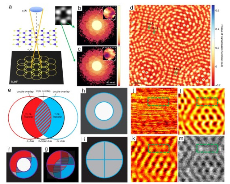
(a) The basic configuration of the defocus ptychography imaging. (b, c) Converging beam electron diffraction pattern at two locations next to the atomic column, inset showing the intensity distribution inside the bright-field disk. (d) Phase contrast image of bilayer MoS2 reconstructed by electron ptychography imaging technique. (e) Schematic of the overlap of the diffractive disks, red and blue represent opposite phases, so only two overlapping regions are non-zero values. (f) The relative distribution of the diffracted disk on the annular brightfield detector. (g) Relative distribution of diffraction Disk on the four-division detector. (h) Annular bright-field detector configuration. (i) Four-division detector configuration. (j) Annular bright-field image of bilayer graphene. (k) Integral phase contrast image of bilayer graphene. (l) SSB-ptychography of bilayer graphene reconstructs phase contrast images. (m) High-angle annular dark-field image of double-layer graphene. The difference in contrast of the green dotted box is obvious. (a–d) Adapted from Springer Nature publisher. (e–m) Adapted from Elsevier publisher.