四维扫描透射电子显微镜技术:从材料微观结构到物性分析
Four-Dimensional Scanning Transmission Electron Microscopy: From Material Microstructures to Physicochemical Properties
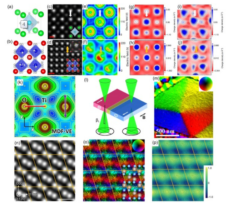
(a) SrTiO3 atomic model. (b) BiFeO3 atomic model. (c) High-angle annular dark field image of SrTiO3. (d) High-angle annular dark-field image of BiFeO3, with inset indicating the offset of Bi atoms. (e) Reconstructed SrTiO3 electric field distribution map. (f) Reconstructed BiFeO3 electric field distribution map. (g) Reconstructed SrTiO3 charge density distribution map. (h) Reconstructed BiFeO3 charge density distribution map. (i) The charge density distribution of SrTiO3 calculated by density functional theory. (j) The charge density distribution of BiFeO3 calculated by density functional theory. (k) Valence electron map of TiO2 aspheric surface. (l) STEM schematic of an electron beam passing through a uniformly magnetized thin film. (m) Color wheel diagram of the magnetic field, showing the direction and magnitude of the magnetic field in the plane. (n) The ADF image of α-Fe2O3 observed along the [${\rm{\bar 1}}$${\rm{\bar 1}}$20] direction. (o) Projected magnetic field vector colour map of α-Fe2O3. The inset color wheel indicates how colour and shade denote the magnetic field orientation and strength in the vector colour map. (p) The magnetic phase-shift image of α-Fe2O3. (a–j) Adapted from Springer Nature publisher. (k) Adapted from Elsevier publisher. (l–m) Adapted from Elsevier publisher. (n–p) Adapted from Springer Nature publisher.