四维扫描透射电子显微镜技术:从材料微观结构到物性分析
Four-Dimensional Scanning Transmission Electron Microscopy: From Material Microstructures to Physicochemical Properties
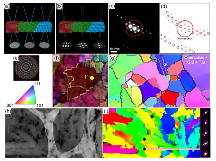
(a) The Kikuchi line was used to determine the crystal orientation. (b) The crystal orientation was determined by the Bragg diffraction point. (c) Crystal diffraction peaks of single crystal silicon under the < 110 > axis. (d) Matching bragg diffraction peaks based on cross-correlation template matching. (e) The Kikuchi diffraction pattern at the yellow dot in (f). (f) Reconstruction of crystal orientation maps of tungsten films using the Kikuchi line fitting method. (g) Reconstruction of crystal orientation map of single-crystal silicon thin films by the method of calibrating Bragg diffraction points. (h) Annular dark field image of the thin film. (i) The crystal orientation distribution map corresponding to the region in Fig.(h). The right side is the diffraction pattern in the corresponding marked range. (a, b) Adapted from Cambridge University Press publisher. (c, d) Adapted from Elsevier publisher. (e, f) Adapted from Cambridge University Press publisher. (g) Adapted from Cambridge University Press publisher. (h, i) Adapted from Springer Nature publisher.