四维扫描透射电子显微镜技术:从材料微观结构到物性分析
Four-Dimensional Scanning Transmission Electron Microscopy: From Material Microstructures to Physicochemical Properties
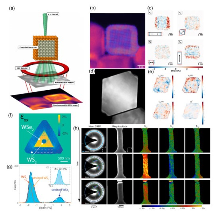
(a) Experimental configuration of the nanobeam electron diffraction. (b) Image of Rh@Pt nanocube after correction the scan distortion and the corrected scan positions are marked as blue dots (c) Mapping of normal and shear strains of Rh@Pt nanocubes, the lower left corner of each strain diagram represents the geometric interpretation of strain formation. (d) Image of Pd@Pt core-shell nanoparticles. (e) Mapping of normal strain and shear strain of Pd@Pt core-shell nanoparticles. (f) Uniaxial strain map. (g) Strain histogram from (f). The inset shows the histogram from a flat region (gray box in panel f) indicating a precision better than ∼0.18%. (h) The average diffraction pattern and a virtual dark-field image are shown along with the color-coded strain maps. Three time resolved maps are shown. The sample is deformed under continuous loading before showing catastrophic fractur. (a–c) Adapted from American Chemical Society publisher. (d, e) Adapted from Elsevier publisher. (f, g) Adapted from American Chemical Society publisher. (h) Adapted from AIP Publishing publisher.