

物理化学学报 >> 2023, Vol. 39 >> Issue (10): 2306043.doi: 10.3866/PKU.WHXB202306043
所属专题: 北大纳米化学研究中心30周年专刊
于梦诗, 谭聪伟, 高啸寅, 唐浚川, 彭海琳( )
)
收稿日期:2023-06-26
录用日期:2023-07-21
发布日期:2023-08-07
通讯作者:
彭海琳
E-mail:hlpeng@pku.edu.cn
作者简介:第一联系人:†These authors contributed equally to this work.
基金资助:
Mengshi Yu, Congwei Tan, Xiaoyin Gao, Junchuan Tang, Hailin Peng()
Received:2023-06-26
Accepted:2023-07-21
Published:2023-08-07
Contact:
Hailin Peng
E-mail:hlpeng@pku.edu.cn
Supported by:摘要:
高迁移率二维半导体材料具有独特的性质,可在原子级厚度下维持晶体管的尺寸微缩,抑制短沟道效应,被认为是“后摩尔时代”晶体管沟道的候选材料。作为二维半导体中的一员,环境稳定、带隙合适的Bi2O2Se备受关注。与其他二维材料不同的是,Bi2O2Se可以通过逐层氧化成高介电常数的氧化物介电层,同时保持原子级平整的界面,这可与半导体产业界中的Si/SiO2相比拟。上述特性使Bi2O2Se成为构筑高性能电子、光电子器件的理想材料平台。为了实现二维Bi2O2Se的广泛应用,开发大面积、高质量、低成本的制备方法至关重要。在这篇综述中,我们总结了通过化学气相沉积方法控制二维Bi2O2Se生长的最新进展。我们首先介绍了Bi2O2Se的晶体结构和性质,而后,我们重点关注二维Bi2O2Se的形貌控制与规则阵列构筑,其中形貌控制包括成核模式的控制与维度控制。此外,我们探讨了通过控制缺陷和释放应力以提高Bi2O2Se电学质量的方法。最后,为满足先进电子应用的需求,我们提出了精确控制Bi2O2Se结构和质量的策略。
于梦诗, 谭聪伟, 高啸寅, 唐浚川, 彭海琳. 高迁移率二维半导体Bi2O2Se的化学气相沉积生长:可控生长及材料质量[J]. 物理化学学报, 2023, 39(10), 2306043. doi: 10.3866/PKU.WHXB202306043
Mengshi Yu, Congwei Tan, Xiaoyin Gao, Junchuan Tang, Hailin Peng. Chemical Vapor Deposition Growth of High-Mobility 2D Semiconductor Bi2O2Se: Controllability and Material Quality[J]. Acta Phys. -Chim. Sin. 2023, 39(10), 2306043. doi: 10.3866/PKU.WHXB202306043
Fig 1
Superior properties of 2D semiconductor Bi2O2Se. (a) Lattice and electronic band structure of Bi2O2Se. Bi2O2Se has a tetragonal structure (I4/mmm) with alternated positively charged [Bi2O2]n2n+ and negatively charged [Se]n2n− layers along the c-axis. It also exhibits zipper-like structure when exfoliated from bulk, leading to Se and Se-vacancy dimers at the surface. Bi2O2Se and its high-κ native-oxide Bi2SeO5 form atomically smooth interface. Electrically, Bi2O2Se is an indirect semiconductor with a band gap of about 0.8 eV. (b) Comparison of effective mass and band gap of 3D and 2D materials, illustrating that Bi2O2Se has a moderate band gap and small effective mass. The data are from Refs. 6,34−56. (c) Comparison of carrier mobility as a function of channel thickness of various semiconductors, showing Bi2O2Se has high mobility without severe degradation as the thickness shrinks. The data are from Refs. 6,33,35,39,50,57−76."
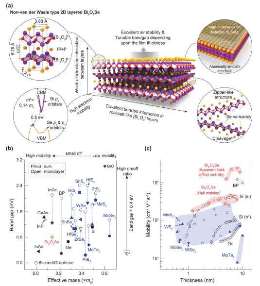
Fig 2
Systematic design and control of chemical vapor deposition (CVD) synthesis of 2D Bi2O2Se. The Bi-O-Se ternary phase diagram (left) indicates the potential precursors to synthesize Bi2O2Se. The key parameters, such as precursor type, growth temperature and substrate engineering, collectively affect CVD growing process (middle). They can further control the nucleation and quality of the products, resulting in different nucleation modes, which includes in-plane epitaxy of 2D nanoplate and film, vertical epitaxy of 2D fins and out-of-plane free-standing nanostructures (right)."
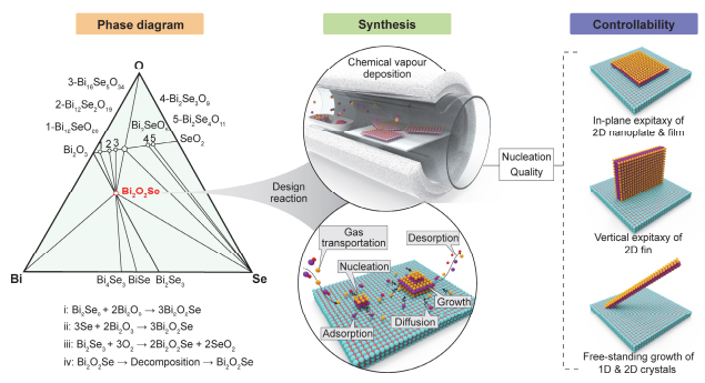
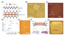
Fig 3
Controlled CVD synthesis of 2D Bi2O2Se on mica. (a) Schematic illustration of Van der Waals epitaxy between Bi2O2Se and mica 83. Adapted from John Wiley and Sons publisher. (b) Optical image of as-synthesized Bi2O2Se nanoplates on mica. Adapted with permission from Ref. 6, Copyright 2017 Springer Nature publisher. (c) AFM image of monolayer Bi2O2Se nanoplates, suggesting the thickness control of 2D Bi2O2Se can be achieved. Adapted with permission from Ref. 80, Copyright 2017 American Chemical Society publisher. (d) Statistics of growth rate and domain size of 2D Bi2O2Se with different growth temperatures. (e) Typical optical image of large-size single-crystal 2D Bi2O2Se up to 2 mm 22. Adapted from John Wiley and Sons publisher. (f) Schematic illustration of the two-stage reverse-flow-assisted CVD process. Stage I involves the reverse flow from valve A to valve B during the beginning temperature ramping stage. Stage Ⅱ involves the gas flow from C to D, carrying vaporized Bi2O2Se. (g) Typical image of a large-size Bi2O2Se single crystal with 750 μm in length and 8.3 nm thickness. (f–g) Adapted with permission from Ref. 81, Copyright 2021 American Chemical Society publisher."
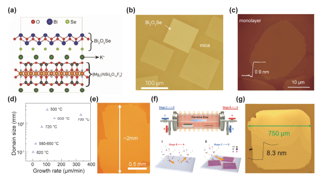
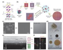
Fig 4
Wafer-scale CVD synthesis of 2D Bi2O2Se on perovskite oxides. (a) Lattice structure of Bi2O2Se and perovskite oxides. (b) Schematic illustration of wafer-scale synthesis of 2D Bi2O2Se via Van der Waals epitaxy between Bi2O2Se and perovskite oxides with excellent lattice and symmetry matching, including (ⅰ) oriented nucleation, (ⅱ) boundary-free growth. (c) SEM images of Bi2O2Se crystals with different growth time of ~5, ~10 and ~20 min, respectively, showing the evolution of Bi2O2Se from single-oriented domains to uniform continuous single-crystal thin films. (d) Photograph of wafer-scale Bi2O2Se thin films grown on several perovskite oxide substrates (2-inch (La, Sr) (Al, Ta)O3, 1-inch LaAlO3, 1-inch SrTiO3, and 1.5 cm × 1.5 cm SrTiO3) with controlled thickness from few layers to 30 nm. (e) Atomic-resolution cross-sectional STEM-HAADF image (left) and corresponding lattice illustration (right) of Bi2O2Se/ SrTiO3 interface, showing perfect epitaxy and single crystallinity. (f) Fast Fourier transformation (FFT) image of e, showing diffraction patterns of Bi2O2Se and SrTiO3. (a–f) Adapted with permission from Ref. 23, Copyright 2019 American Chemical Society publisher."

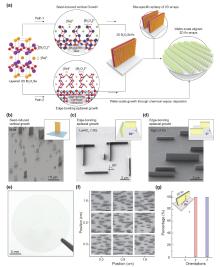
Fig 5
Controlled CVD synthesis of vertical Bi2O2Se fins. (a) Schematic illustration of two approaches to synthesizing vertical Bi2O2Se fins: (ⅰ) seed-induced vertical growth, (ⅱ) edge-bonding epitaxial growth. Subsequently, site-specific vertical growth can be designed to achieve wafer-scale aligned 2D fin arrays. (b) SEM image of seed-induced vertical growth of Bi2O2Se fins on mica 83. Inset: schematic of 2D fin on mica. Adapted from John Wiley and Sons publisher. (c) Tilted SEM image of edge-bonding epitaxial growth of Bi2O2Se fins on LaAlO3 (100) surface. Inset: schematic of two perpendicular orientations of 2D fins on 4-fold symmetry LaAlO3 (100) surface. (d) Tilted SEM image of edge-bonding epitaxial growth of unidirectionally aligned Bi2O2Se fins on MgO (110) surface. Inset: schematic of single orientation of 2D fins on 2-fold symmetry MgO (110) surface. (e) Optical image of the vertical 2D fin arrays wafer. (f) Typical SEM images of aligned vertical 2D Bi2O2Se fin arrays on the 1-inch MgO (110) wafer (1.8 cm × 1.8 cm). (g) Orientation distribution of vertical 2D Bi2O2Se fin arrays on the wafer. Inset: schematic for the 2D Bi2O2Se fin orientation on epitaxy substrate. (c–g) Adapted with permission from Ref. 7, Copyright 2023 Springer Nature publisher."
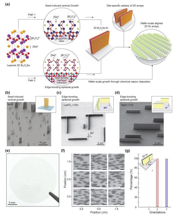
Fig 6
Dimensionality control of Bi2O2Se via CVD synthesis. (a) Schematic illustration of dimension control of Bi2O2Se: (ⅰ) square nanoplates via isotropic growth; (ⅱ) 1D nanoribbons via anisotropic growth. Adapted from Acta Physico-Chimica Sinica publisher. (b) Dimensional phase diagram of Bi2O2Se, determined by Bi2O3/Bi2Se3 ratio and growth temperature collectively 77. Inset, typical optical images of square shape Bi2O2Se and Bi2O2Se nanoribbons. Adapted from John Wiley and Sons publisher. (c, d) Typical SEM images of 1D nanoribbons via epitaxial growth (c) and vapor-liquid-solid (VLS) growth (d), respectively. (c) Adapted with permission from Ref. 84, Copyright 2019 AIP publishing. (d) Adapted with permission from Ref. 85, Copyright 2019 American Physical Society publisher. (e) Length and width control of 1D Bi2O2Se nanoribbons. Adapted with permission from Ref. 86, Copyright 2020 Acta Physico-Chimica Sinica publisher. (f, g) Thickness control of 1D Bi2O2Se nanoribbons, showing both monolayer (f) and multilayer (g) nanoribbons can be synthesized 77. Adapted from John Wiley and Sons publisher."
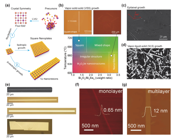
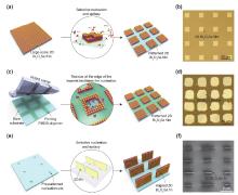
Fig 7
Approaches for preparing ordered 2D Bi2O2Se arrays. (a, b) Illustration of selective-area chemical etching to prepare ordered 2D Bi2O2Se crystal arrays (a) and the optical microscopic (OM) image of corresponding result (b) 88. (b) Adapted from John Wiley and Sons publisher. (c, d) Illustration of selective-area growth for the preparation of ordered 2D Bi2O2Se crystal arrays via pretreatment of substrate (c) and the optical microscopic (OM) image of corresponding result (d) 80. (d) Adapted from American Chemical Society publisher. (e, f) Illustration of site-controlled growth for the preparation of ordered 2D Bi2O2Se fin arrays via pre-patterned nucleation sites (e) and the scanning electron microscopy (SEM) image of corresponding result (f) 7. (f) Adapted from Springer Nature publisher."
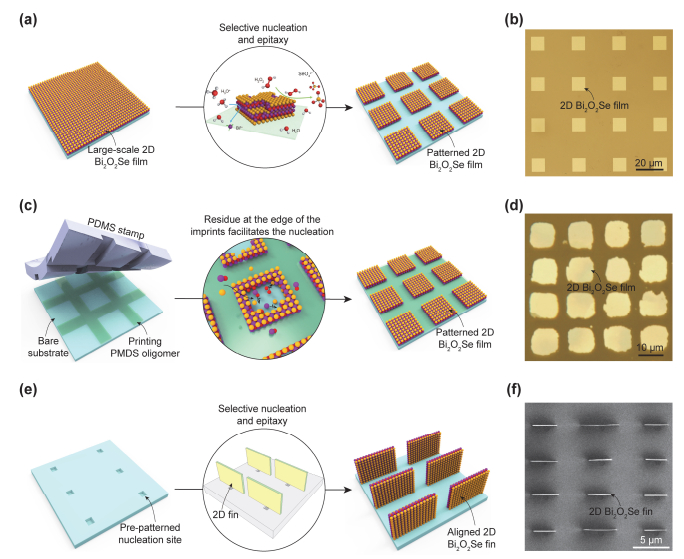
Fig 8
Defect control and self-modulation doping effect of 2D Bi2O2Se via CVD synthesis. (a) Illustration of five possible defects in Bi2O2Se shown by atomic structure. (b) Calculated band structure of 2D Bi2O2Se with VSe defects. Fermi level is at 0 and the red dots show the anticipated bands on the nearest Bi and Se atoms close to the VSe defects. (a, b) Adapted with permission from Ref. 89, Copyright 2018 American Physical Society publisher. (c) Defect transition levels for Bi2O2Se. The blue areas represent conduction and valence bands. The solid and hollow circles show donor and acceptor defects, respectively. Adapted with permission from Ref. 90, Copyright 2018 AIP Publishing. (d) The relation between formation energy for defects in Bi2O2Se and different Se-richness conditions 89. (e) Statistics for Hall mobility at 2 K and residual resistance ratios of Bi2O2Se obtained under Se-rich and Se-poor conditions 89. The plot shows that Bi2O2Se synthesized under Se-poor condition has much higher mobility and residual resistance ratio than under Se-rich condition. (d, e) Adapted from American Physical Society publisher. (f) Comparison of carrier concentration and the corresponding mobility of Bi2O2Se via different growth methods (precursors) 79,81."
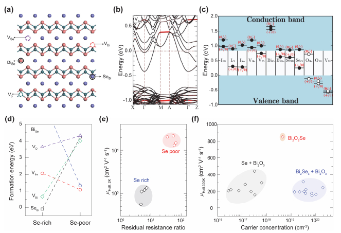
Fig 9
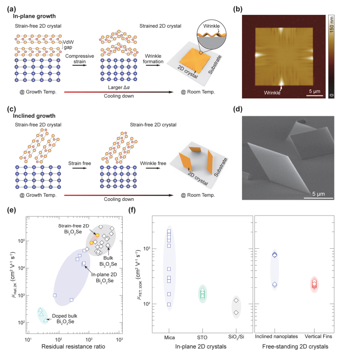
Improved electrical properties of 2D Bi2O2Se via strain-free out-of-plane CVD synthesis. (a, b) Schematic illustration (a) and AFM image (b) of internal strain of in-plane 2D Bi2O2Se nanoplate caused by wrinkles during cooling process after CVD growth. (c, d) Schematic illustration (c) and SEM image (d) of strain-free 2D Bi2O2Se crystals obtained by free-standing CVD synthesis with a self-catalyzed VLS mechanism. (a–c) Adapted with permission from Ref. 51, Copyright 2022 American Chemical Society publisher. (d) Adapted with permission from Ref. 91, Copyright 2020 American Chemical Society publisher. (e) Statistics and contrast of Hall mobility at 2 K and residual resistance ratio of free-standing strain-free Bi2O2Se crystals and previously reported in-plane strained Bi2O2Se nanoplates 51,92. (f) Statistics and contrast of field-effect mobility of free-standing Bi2O2Se crystals 7,51,86,91 and previously reported in-plane strained Bi2O2Se nanoplates 6,8,11,22,23,77,81,93–97."
| 1 |
Kang K. ; Lee K. H. ; Han Y. ; Gao H. ; Xie S. ; Muller D. A. ; Park J. Nature 2017, 550 (7675), 229.
doi: 10.1038/nature23905 |
| 2 |
Liu Y. ; Duan X. ; Shin H.-J. ; Park S. ; Huang Y. ; Duan X. Nature 2021, 591 (7848), 43.
doi: 10.1038/s41586-021-03339-z |
| 3 |
Akinwande D. ; Huyghebaert C. ; Wang C. H. ; Serna M. I. ; Goossens S. ; Li L. J. ; Wong H. P. ; Koppens F. H. L. Nature 2019, 573 (7775), 507.
doi: 10.1038/s41586-019-1573-9 |
| 4 |
Chhowalla M. ; Jena D. ; Zhang H. Nat. Rev. Mater. 2016, 1 (11), 16052.
doi: 10.1038/natrevmats2016.52 |
| 5 |
Wang S. ; Liu X. ; Xu M. ; Liu L. ; Yang D. ; Zhou P. Nat. Mater. 2022, 21, 1225.
doi: 10.1038/s41928-022-00824-9 |
| 6 |
Wu J. ; Yuan H. ; Meng M. ; Chen C. ; Sun Y. ; Chen Z. ; Dang W. ; Tan C. ; Liu Y. ; Yin J. ; et al Nat. Nanotech. 2017, 12, 530.
doi: 10.1038/NNANO.2017.43 |
| 7 |
Tan C. ; Yu M. ; Tang J. ; Gao X. ; Yin Y. ; Zhang Y. ; Wang J. ; Gao X. ; Zhang C. ; Zhou X. ; et al Nature 2023, 616 (7955), 66.
doi: 10.1038/s41586-023-05797-z |
| 8 |
Zhang Y. ; Yu J. ; Zhu R. ; Wang M. ; Tan C. ; Tu T. ; Zhou X. ; Zhang C. ; Yu M. ; Gao X. ; et al Nat. Electron. 2022, 5 (10), 643.
doi: 10.1038/s41928-022-00824-9 |
| 9 |
Li P. ; Han A. ; Zhang C. ; He X. ; Zhang J. ; Zheng D. ; Cheng L. ; Li L.-J. ; Miao G.-X. ; Zhang X.-X. ACS Nano 2020, 14 (9), 11319.
doi: 10.1021/acsnano.0c03346 |
| 10 |
Ying J. ; He J. ; Yang G. ; Liu M. ; Lyu Z. ; Zhang X. ; Liu H. ; Zhao K. ; Jiang R. ; Ji Z. ; et al Nano Lett. 2020, 20 (4), 2569.
doi: 10.1021/acs.nanolett.0c00025 |
| 11 |
Li T. ; Tu T. ; Sun Y. ; Fu H. ; Yu J. ; Xing L. ; Wang Z. ; Wang H. ; Jia R. ; Wu J. ; et al Nat. Electron. 2020, 3, 473.
doi: 10.1038/s41928-020-0444-6 |
| 12 |
Zhang C. ; Tu T. ; Wang J. ; Zhu Y. ; Tan C. ; Chen L. ; Wu M. ; Zhu R. ; Liu Y. ; Fu H. ; et al Nat. Mater. 2023,
doi: 10.1038/s41563-023-01502-7 |
| 13 |
Yang F. ; Wu J. ; Suwardi A. ; Zhao Y. ; Liang B. ; Jiang J. ; Xu J. ; Chi D. ; Hippalgaonkar K. ; Lu J. ; Ni Z. Adv. Mater. 2020, e2004786.
doi: 10.1002/adma.202004786 |
| 14 |
Yin J. ; Tan Z. ; Hong H. ; Wu J. ; Yuan H. ; Liu Y. ; Chen C. ; Tan C. ; Yao F. ; Li T. ; et al Nat. Commun. 2018, 9 (1), 3311.
doi: 10.1038/s41467-018-05874-2 |
| 15 |
Chen Y. ; Ma W. ; Tan C. ; Luo M. ; Zhou W. ; Yao N. ; Wang H. ; Zhang L. ; Xu T. ; Tong T. ; et al Adv. Funct. Mater. 2021, 31 (14)
doi: 10.1002/adfm.202009554 |
| 16 |
Tian X. ; Luo H. ; Wei R. ; Zhu C. ; Guo Q. ; Yang D. ; Wang F. ; Li J. ; Qiu J. Adv. Mater. 2018, 30 (31), 1801021.
doi: 10.1002/adma.201801021 |
| 17 |
Xu S. ; Fu H. ; Tian Y. ; Deng T. ; Cai J. ; Wu J. ; Tu T. ; Li T. ; Tan C. ; Liang Y. ; et al Angew. Chem. Int. Ed. 2020, 59, 17938.
doi: 10.1002/anie.202006745 |
| 18 |
Zhang C. ; Wu J. ; Sun Y. ; Tan C. ; Li T. ; Tu T. ; Zhang Y. ; Liang Y. ; Zhou X. ; Gao P. ; et al J. Am. Chem. Soc. 2020, 142 (6), 2726.
doi: 10.1021/jacs.9b11668 |
| 19 |
Xia Y. ; Wang J. ; Chen R. ; Wang H. ; Xu H. ; Jiang C. ; Li W. ; Xiao X. Adv. Electron. Mater. 2022, 8 (9), 2200126.
doi: 10.1002/aelm.202200126 |
| 20 |
Liu B. ; Zhao Y. ; Verma D. ; Wang L. A. ; Liang H. ; Zhu H. ; Li L. J. ; Hou T. H. ; Lai C. S. ACS Appl. Mater. Interfaces 2021, 13, 15391.
doi: 10.1021/acsami.1c00177 |
| 21 |
Zhang Z. ; Li T. ; Wu Y. ; Jia Y. ; Tan C. ; Xu X. ; Wang G. ; Lv J. ; Zhang W. ; He Y. ; et al Adv. Mater. 2019, 31 (3), 1805769.
doi: 10.1002/adma.201805769 |
| 22 |
Khan U. ; Luo Y. ; Tang L. ; Teng C. ; Liu J. ; Liu B. ; Cheng H. M. Adv. Funct. Mater. 2019, 29 (14), 1807979.
doi: 10.1002/adfm.201807979 |
| 23 |
Tan C. ; Tang M. ; Wu J. ; Liu Y. ; Li T. ; Liang Y. ; Deng B. ; Tan Z. ; Tu T. ; Zhang Y. ; et al Nano Lett. 2019, 19 (3), 2148.
doi: 10.1021/acs.nanolett.9b00381 |
| 24 |
Liang Y. ; Chen Y. ; Sun Y. ; Xu S. ; Wu J. ; Tan C. ; Xu X. ; Yuan H. ; Yang L. ; Chen Y. ; et al Adv. Mater. 2019, 31 (39), 1901964.
doi: 10.1002/adma.201901964 |
| 25 |
Song Y. ; Li Z. ; Li H. ; Tang S. ; Mu G. ; Xu L. ; Peng W. ; Shen D. ; Chen Y. ; Xie X. ; et al Nanotechnology 2020, 31 (16), 165704.
doi: 10.1088/1361-6528/ab6686 |
| 26 |
Kang M. ; Chai H. J. ; Jeong H. B. ; Park C. ; Jung I. Y. ; Park E. ; Cicek M. M. ; Lee I. ; Bae B. S. ; Durgun E. ; et al ACS Nano 2021, 15 (5), 8715.
doi: 10.1021/acsnano.1c00811 |
| 27 |
Dang L. Y. ; Liu M. ; Wang G. G. ; Zhao D. Q. ; Han J. C. ; Zhu J. Q. ; Liu Z. Adv. Funct. Mater. 2022, 32 (31), 2201020.
doi: 10.1002/adfm.202201020 |
| 28 |
Li M. Q. ; Dang L. Y. ; Wang G. G. ; Li F. ; Han M. ; Wu Z. P. ; Li G. Z. ; Liu Z. ; Han J. C. Adv. Mater. Technol. 2020, 5 (7), 2000180.
doi: 10.1002/admt.202000180 |
| 29 |
Wei Q. ; Li R. ; Lin C. ; Han A. ; Nie A. ; Li Y. ; Li L. J. ; Cheng Y. ; Huang W. ACS Nano 2019, 13 (11), 13439.
doi: 10.1021/acsnano.9b07000 |
| 30 |
Chen C. ; Wang M. ; Wu J. ; Fu H. ; Yang H. ; Tian Z. ; Tu T. ; Peng H. ; Sun Y. ; Xu X. ; et al Sci. Adv. 2018, 4 (9), eaat8355.
doi: 10.1126/sciadv.aat8355 |
| 31 |
Eremeev S. V. ; Koroteev Y. M. ; Chulkov E. V. Phys. Rev. B 2019, 100 (11)
doi: 10.1103/PhysRevB.100.115417 |
| 32 |
Meng M. ; Huang S. ; Tan C. ; Wu J. ; Jing Y. ; Peng H. ; Xu H. Nanoscale 2018, 10, 2704.
doi: 10.1039/C7NR08874D |
| 33 |
Zhou X. ; Liang Y. ; Fu H. ; Zhu R. ; Wang J. ; Cong X. ; Tan C. ; Zhang C. ; Zhang Y. ; Wang Y. ; et al Adv. Mater. 2022, 34 (42), e2202754.
doi: 10.1002/adma.202202754 |
| 34 | Li X. ; Yu Z. ; Xiong X. ; Li T. ; Gao T. ; Wang R. ; Huang R. ; Wu Y. Sci. Adv. 2019, 5 (6), eaau3194. |
| 35 |
Radisavljevic B. ; Radenovic A. ; Brivio J. ; Giacometti V. ; Kis A. Nat. Nanotechnol. 2011, 6 (3), 147.
doi: 10.1038/nnano.2010.279 |
| 36 |
Tongay S. ; Zhou J. ; Ataca C. ; Lo K. ; Matthews T. S. ; Li J. ; Grossman J. C. ; Wu J. Nano Lett. 2012, 12 (11), 5576.
doi: 10.1021/nl302584w |
| 37 |
Yun W. S. ; Han S. W. ; Hong S. C. ; Kim I. G. ; Lee J. D. Phys. Rev. B 2012, 85 (3), 033305.
doi: 10.1103/PhysRevB.85.033305 |
| 38 |
Zhao Y. ; Qiao J. ; Yu P. ; Hu Z. ; Lin Z. ; Lau S. P. ; Liu Z. ; Ji W. ; Chai Y. Adv. Mater. 2016, 28 (12), 2399.
doi: 10.1002/adma.201504572 |
| 39 |
Iqbal M. W. ; Iqbal M. Z. ; Khan M. F. ; Shehzad M. A. ; Seo Y. ; Park J. H. ; Hwang C. ; Eom J. Sci. Rep. 2015, 5, 10699.
doi: 10.1038/srep10699 |
| 40 |
Yang C.-x. ; Zhao X. ; Wei S.-y. Solid State Commun. 2016, 245, 70.
doi: 10.1016/j.ssc.2016.07.003 |
| 41 |
Brotons-Gisbert M. ; Andres-Penares D. ; Suh J. ; Hidalgo F. ; Abargues R. ; Rodriguez-Canto P. J. ; Segura A. ; Cros A. ; Tobias G. ; Canadell E. ; et al Nano Lett. 2016, 16 (5), 3221.
doi: 10.1021/acs.nanolett.6b00689 |
| 42 |
Gonzalez J. M. ; Oleynik I. I. Phys. Rev. B 2016, 94 (12), 125443.
doi: 10.1103/PhysRevB.94.125443 |
| 43 |
Novoselov K. S. ; Geim A. K. ; Morozov S. V. ; Jiang D. ; Katsnelson M. I. ; Grigorieva I. V. ; Dubonos S. V. ; Firsov A. A. Nature 2005, 438 (7065), 197.
doi: 10.1038/nature04233 |
| 44 |
Ni Z. ; Liu Q. ; Tang K. ; Zheng J. ; Zhou J. ; Qin R. ; Gao Z. ; Yu D. ; Lu J. Nano Lett. 2012, 12 (1), 113.
doi: 10.1021/nl203065e |
| 45 |
Zhao Q. ; Guo Y. ; Si K. ; Ren Z. ; Bai J. ; Xu X. Phys. Status. Solidi. (b) 2017, 254 (9), 1700033.
doi: 10.1002/pssb.201700033 |
| 46 | Sze S. M. ; Ng K. K. Physics of Semiconductor Devices New Jersey, USA: John Wiley & Sons, 2006, pp. 5- 75. |
| 47 |
Mu X. ; Wang J. ; Sun M. Mat. Today Phys 2019, 8, 92.
doi: 10.1016/j.mtphys.2019.02.003 |
| 48 |
Cheng L. ; Liu Y. J. Am. Chem. Soc. 2018, 140 (51), 17895.
doi: 10.1021/jacs.8b07871 |
| 49 |
Caruso F. ; Amsalem P. ; Ma J. ; Aljarb A. ; Schultz T. ; Zacharias M. ; Tung V. ; Koch N. ; Draxl C. Phys. Rev. B 2021, 103 (20), 205152.
doi: 10.1103/PhysRevB.103.205152 |
| 50 |
Keum D. H. ; Cho S. ; Kim J. H. ; Choe D.-H. ; Sung H.-J. ; Kan M. ; Kang H. ; Hwang J.-Y. ; Kim S. W. ; Yang H. ; et al Nat. Phys. 2015, 11 (6), 482.
doi: 10.1038/nphys3314 |
| 51 |
Tan C. ; Jiang J. ; Wang J. ; Yu M. ; Tu T. ; Gao X. ; Tang J. ; Zhang C. ; Zhang Y. ; Zhou X. ; et al Nano Lett. 2022, 22 (9), 3770.
doi: 10.1021/acs.nanolett.2c00820 |
| 52 |
Chen X. ; Chen C. ; Levi A. ; Houben L. ; Deng B. ; Yuan S. ; Ma C. ; Watanabe K. ; Taniguchi T. ; Naveh D. ; et al ACS Nano 2018, 12 (5), 5003.
doi: 10.1021/acsnano.8b02295 |
| 53 |
Dorgan V. E. ; Bae M.-H. ; Pop E. Appl. Phys. Lett. 2010, 97 (8), 082112.
doi: 10.1063/1.3483130 |
| 54 |
Smithe K. K. H. ; English C. D. ; Suryavanshi S. V. ; Pop E. Nano Lett. 2018, 18 (7), 4516.
doi: 10.1021/acs.nanolett.8b01692 |
| 55 |
Jin Z. ; Li X. ; Mullen J. T. ; Kim K. W. Phys. Rev. B 2014, 90 (4), 045422.
doi: 10.1103/PhysRevB.90.045422 |
| 56 |
Rengel R. ; Iglesias J. M. ; Hamham E. M. ; Martín M. J. Semicond. Sci. Tech. 2018, 33 (6), 065011.
doi: 10.1088/1361-6641/aac0a2 |
| 57 |
Xu Y. ; Shi X. ; Zhang Y. ; Zhang H. ; Zhang Q. ; Huang Z. ; Xu X. ; Guo J. ; Zhang H. ; Sun L. ; et al Nat. Commun. 2020, 11 (1), 1330.
doi: 10.1038/s41467-020-14902-z |
| 58 |
Li L. ; Yu Y. ; Ye G. J. ; Ge Q. ; Ou X. ; Wu H. ; Feng D. ; Chen X. H. ; Zhang Y. Nat. Nanotechnol. 2014, 9 (5), 372.
doi: 10.1038/nnano.2014.35 |
| 59 | Chang, W. H.; Irisawa, T.; Ishii, H.; Hattori, H.; Uchida, N.; Maeda, T. In HEtero-layer-lift-off (HELLO) technology for enhanced hole mobility in UTB GeOI pMOSFETs, 2018 International Symposium on VLSI Technology, Systems and Application (VLSI-TSA), Hsinchu, Taiwan, 16–19 April 2018; 2018; pp. 1–2. |
| 60 |
Zhu W. ; Perebeinos V. ; Freitag M. ; Avouris P. Phys. Rev. B 2009, 80 (23), 235402.
doi: 10.1103/PhysRevB.80.235402 |
| 61 |
Kanazawa T. ; Amemiya T. ; Ishikawa A. ; Upadhyaya V. ; Tsuruta K. ; Tanaka T. ; Miyamoto Y. Sci. Rep. 2016, 6, 22277.
doi: 10.1038/srep22277 |
| 62 |
Mleczko M. J. ; Zhang C. ; Lee H. R. ; Kuo H.-H. ; Magyari-Köpe B. ; Moore R. G. ; Shen Z.-X. ; Fisher I. R. ; Nishi Y. ; Pop E. Sci. Adv. 2017, 3 (8), e1700481.
doi: 10.1126/sciadv.1700481 |
| 63 |
English C. D. ; Shine G. ; Dorgan V. E. ; Saraswat K. C. ; Pop E. Nano Lett. 2016, 16 (6), 3824.
doi: 10.1021/acs.nanolett.6b01309 |
| 64 |
Cheng R. ; Jiang S. ; Chen Y. ; Liu Y. ; Weiss N. ; Cheng H. C. ; Wu H. ; Huang Y. ; Duan X. Nat. Commun. 2014, 5, 5143.
doi: 10.1038/ncomms6143 |
| 65 |
Li T. ; Guo W. ; Ma L. ; Li W. ; Yu Z. ; Han Z. ; Gao S. ; Liu L. ; Fan D. ; Wang Z. ; et al Nat. Nanotechnol. 2021, 16 (11), 1201.
doi: 10.1038/s41565-021-00963-8 |
| 66 |
Liu L. ; Li T. ; Ma L. ; Li W. ; Gao S. ; Sun W. ; Dong R. ; Zou X. ; Fan D. ; Shao L. ; et al Nature 2022, 605 (7908), 69.
doi: 10.1038/s41586-022-04523-5 |
| 67 |
Larentis S. ; Fallahazad B. ; Tutuc E. Appl. Phys. Lett. 2012, 101 (22), 223104.
doi: 10.1063/1.4768218 |
| 68 |
Ji H. ; Joo M. K. ; Yi H. ; Choi H. ; Gul H. Z. ; Ghimire M. K. ; Lim S. C. ACS Appl. Mater. Interfaces 2017, 9 (34), 29185.
doi: 10.1021/acsami.7b05865 |
| 69 |
Zhao Y. ; Qiao J. ; Yu Z. ; Yu P. ; Xu K. ; Lau S. P. ; Zhou W. ; Liu Z. ; Wang X. ; Ji W. ; et al Adv. Mater. 2017, 29 (5), 1604230.
doi: 10.1002/adma.201604230 |
| 70 | Uchida, K.; Watanabe, H.; Kinoshita, A.; Koga, J.; Numata, T.; Takagi, S. In Experimental Study on Carrier Transport Mechanism in Ultrathin-body SOI n- and p-MOSFETs with SOI Thickness Less Than 5 nm. International Electron Devices Meeting, San Francisco, CA, USA, 8–11 Dec. 2002; 2002; pp. 47–50. |
| 71 | Irisawa, T.; Numata, T.; Tezuka, T.; Sugiyama, N.; Takagi, S. I. In Electron Transport Properties of Ultrathin-body and Tri-gate SOI nMOSFETs with Biaxial and Uniaxial Strain, International Electron Devices Meeting, San Francisco, CA, USA, 11–13 Dec. 2006; 2006; pp. 1–4. |
| 72 |
Song H. S. ; Li S. L. ; Gao L. ; Xu Y. ; Ueno K. ; Tang J. ; Cheng Y. B. ; Tsukagoshi K. Nanoscale 2013, 5 (20), 9666.
doi: 10.1039/c3nr01899g |
| 73 |
Aji A. S. ; Solís-Fernández P. ; Ji H. G. ; Fukuda K. ; Ago H. Adv. Funct. Mater. 2017, 27 (47), 1703448.
doi: 10.1002/adfm.201703448 |
| 74 |
Pudasaini P. R. ; Oyedele A. ; Zhang C. ; Stanford M. G. ; Cross N. ; Wong A. T. ; Hoffman A. N. ; Xiao K. ; Duscher G. ; Mandrus D. G. ; et al Nano Res. 2017, 11 (2), 722.
doi: 10.1007/s12274-017-1681-5 |
| 75 |
Pradhan N. R. ; Rhodes D. ; Memaran S. ; Poumirol J. M. ; Smirnov D. ; Talapatra S. ; Feng S. ; Perea-Lopez N. ; Elias A. L. ; Terrones M. ; et al Sci. Rep. 2015, 5, 8979.
doi: 10.1038/srep08979 |
| 76 |
Ji H. G. ; Solis-Fernandez P. ; Yoshimura D. ; Maruyama M. ; Endo T. ; Miyata Y. ; Okada S. ; Ago H. Adv. Mater. 2019, 31 (42), 1903613.
doi: 10.1002/adma.201903613 |
| 77 |
Khan U. ; Tang L. ; Ding B. ; Yuting L. ; Feng S. ; Chen W. ; Khan M. J. ; Liu B. ; Cheng H. M. Adv. Funct. Mater. 2021, 31 (31), 2101170.
doi: 10.1002/adfm.202101170 |
| 78 |
Wei Y. ; Chen C. ; Tan C. ; He L. ; Ren Z. ; Zhang C. ; Peng S. ; Han J. ; Zhou H. ; Wang J. Adv. Opt. Mater. 2022, 10 (23), 2201396.
doi: 10.1002/adom.202201396 |
| 79 |
Wu J. ; Qiu C. ; Fu H. ; Chen S. ; Zhang C. ; Dou Z. ; Tan C. ; Tu T. ; Li T. ; Zhang Y. ; et al Nano Lett 2019, 19 (1), 197.
doi: 10.1021/acs.nanolett.8b03696 |
| 80 |
Wu J. ; Tan C. ; Tan Z. ; Liu Y. ; Yin J. ; Dang W. ; Wang M. ; Peng H. Nano Lett. 2017, 17, 3021.
doi: 10.1021/acs.nanolett.7b00335 |
| 81 |
Yang X. ; Zhang Q. ; Song Y. ; Fan Y. ; He Y. ; Zhu Z. ; Bai Z. ; Luo Q. ; Wang G. ; Peng G. ; et al ACS Appl. Mater. Interfaces 2021, 13 (41), 49153.
doi: 10.1021/acsami.1c13491 |
| 82 |
Qin B. ; Saeed M. Z. ; Li Q. ; Zhu M. ; Feng Y. ; Zhou Z. ; Fang J. ; Hossain M. ; Zhang Z. ; Zhou Y. ; et al Nat. Commun. 2023, 14 (1), 304.
doi: 10.1038/s41467-023-35983-6 |
| 83 |
Wu Z. ; Liu G. ; Wang Y. ; Yang X. ; Wei T. ; Wang Q. ; Liang J. ; Xu N. ; Li Z. ; Zhu B. ; et al Adv. Funct. Mater. 2019, 29 (50), 1906639.
doi: 10.1002/adfm.201906639 |
| 84 |
Li J. ; Wang Z. ; Chu J. ; Cheng Z. ; He P. ; Wang J. ; Yin L. ; Cheng R. ; Li N. ; Wen Y. ; et al Appl. Phys. Lett. 2019, 114 (15), 151104.
doi: 10.1063/1.5094192 |
| 85 |
Ying J. ; Yang G. ; Lyu Z. ; Liu G. ; Ji Z. ; Fan J. ; Yang C. ; Jing X. ; Yang H. ; Lu L. ; et al Phys. Rev. B 2019, 100 (23), 235307.
doi: 10.1103/PhysRevB.100.235307 |
| 86 | Tan C. ; Yu M. ; Xu S. ; Wu J. ; Chen S. ; Zhao Y. ; Liu C. ; Zhang Y. ; Tu T. ; Li T. ; et al Acta Phys. -Chim. Sin. 2020, 36 (1), 1908038. |
|
谭聪伟; 于梦诗; 许适溥; 吴金雄; 陈树林; 赵艳; 刘聪; 张亦弛; 涂腾; 李天然; 等. 物理化学学报, 2020, 36 (1), 1908038.
doi: 10.3866/PKU.WHXB201908038 |
|
| 87 |
Li T. ; Peng H. Acc. Mater. Res. 2021, 2 (9), 842.
doi: 10.1021/accountsmr.1c00130 |
| 88 |
Wu J. ; Liu Y. ; Tan Z. ; Tan C. ; Yin J. ; Li T. ; Tu T. ; Peng H. Adv. Mater. 2017, 29, 1704060.
doi: 10.1002/adma.201704060 |
| 89 |
Fu H. ; Wu J. ; Peng H. ; Yan B. Phys. Rev. B 2018, 97 (24), 241203.
doi: 10.1103/PhysRevB.97.241203 |
| 90 |
Wei Q. ; Lin C. ; Li Y. ; Zhang X. ; Zhang Q. ; Shen Q. ; Cheng Y. ; Huang W. J. Appl. Phys. 2018, 124 (5), 055701.
doi: 10.1063/1.5040690 |
| 91 |
Hong C. ; Tao Y. ; Nie A. ; Zhang M. ; Wang N. ; Li R. ; Huang J. ; Huang Y. ; Ren X. ; Cheng Y. ; et al ACS Nano 2020, 14, 16803.
doi: 10.1021/acsnano.0c05300 |
| 92 |
Wang J. ; Wu J. ; Wang T. ; Xu Z. ; Wu J. ; Hu W. ; Ren Z. ; Liu S. ; Behnia K. ; Lin X. Nat. Commun. 2020, 11 (1), 3846.
doi: 10.1038/s41467-020-17692-6 |
| 93 |
Khan U. ; Nairan A. ; Khan K. ; Li S. ; Liu B. ; Gao J. Small 2022, 19 (10), 2206648.
doi: 10.1002/smll.202206648 |
| 94 |
Tong T. ; Chen Y. ; Qin S. ; Li W. ; Zhang J. ; Zhu C. ; Zhang C. ; Yuan X. ; Chen X. ; Nie Z. ; et al Adv. Funct. Mater. 2019, 29 (50), 1905806.
doi: 10.1002/adfm.201905806 |
| 95 |
Zhao K. ; Liu H. ; Tan C. ; Xiao J. ; Shen J. ; Liu G. ; Peng H. ; Lu L. ; Qu F. Appl. Phys. Lett. 2022, 121 (21), 212104.
doi: 10.1063/5.0126739 |
| 96 |
Zou X. ; Sun Y. ; Wang C. Small Methods 2022, 6 (8), 2200347.
doi: 10.1002/smtd.202200347 |
| 97 |
Sagar R. U. R. ; Khan U. ; Galluzzi M. ; Aslam S. ; Nairan A. ; Anwar T. ; Ahmad W. ; Zhang M. ; Liang T. ACS Appl. Electron. Mater. 2020, 2 (7), 2123.
doi: 10.1021/acsaelm.0c00344 |
| [1] | 贺梦菲, 陈超, 唐月, 孟思, 王遵法, 王立煜, 行家宝, 张欣宇, 黄佳慧, 卢江波, 井红梅, 刘翔宇, 徐华. 外延生长具有厚度可调导电属性的非层状二维碲化锰纳米片用于p-型场效应晶体管和优异的接触电极[J]. 物理化学学报, 2025, 41(2): 100016 - . |
| [2] | 张城城, 吴之怡, 沈家辉, 何乐, 孙威. 硅纳米结构阵列:光热CO2催化的新兴平台[J]. 物理化学学报, 2024, 40(1): 2304004 - . |
| [3] | 张婧雯, 马华隆, 马军, 胡梅雪, 李启浩, 陈胜, 宁添姝, 葛创新, 刘晰, 肖丽, 庄林, 张熠霄, 陈立桅. 碱性聚合物电解质膜的表面锥形阵列结构提升燃料电池性能[J]. 物理化学学报, 2023, 39(2): 2111037 -0 . |
| [4] | 吴倩, 高庆平, 单彬, 王文政, 齐玉萍, 台夕市, 王霞, 郑冬冬, 严虹, 应斌武, 罗永嵩, 孙圣钧, 刘倩, Hamdy Mohamed S., 孙旭平. 自支撑过渡金属海水电解析氧催化剂研究进展[J]. 物理化学学报, 2023, 39(12): 2303012 - . |
| [5] | 亓月, 孙禄钊, 刘忠范. 超级蒙烯材料:石墨烯家族的新成员[J]. 物理化学学报, 2023, 39(10): 2307028 - . |
| [6] | 刘若娟, 刘冰之, 孙靖宇, 刘忠范. 气相助剂辅助绝缘衬底上石墨烯生长:现状与展望[J]. 物理化学学报, 2023, 39(1): 2111011 -0 . |
| [7] | 张则尧, 姚艺希, 李彦. FeCo/MgO催化生长体相单壁碳纳米管的直径调控[J]. 物理化学学报, 2022, 38(8): 2101055 - . |
| [8] | 邹菁云, 高冰, 张小品, 唐磊, 冯思敏, 金赫华, 刘碧录, 成会明. 一维碳纳米管/二维二硫化钼混合维度异质结的原位制备及其电荷转移性能[J]. 物理化学学报, 2022, 38(5): 2008037 - . |
| [9] | 程熠, 王坤, 亓月, 刘忠范. 石墨烯纤维材料的化学气相沉积生长方法[J]. 物理化学学报, 2022, 38(2): 2006046 - . |
| [10] | 姜蓓, 孙靖宇, 刘忠范. 石墨烯晶圆的制备:从高品质到规模化[J]. 物理化学学报, 2022, 38(2): 2007068 - . |
| [11] | 程婷, 孙禄钊, 刘志荣, 丁峰, 刘忠范. 金属衬底在石墨烯化学气相沉积生长中的作用[J]. 物理化学学报, 2022, 38(1): 2012006 - . |
| [12] | 刘晓婷, 张金灿, 陈恒, 刘忠范. 超洁净石墨烯薄膜的制备方法[J]. 物理化学学报, 2022, 38(1): 2012047 - . |
| [13] | 陈恒, 张金灿, 刘晓婷, 刘忠范. 气相反应对CVD生长石墨烯的影响[J]. 物理化学学报, 2022, 38(1): 2101053 - . |
| [14] | 陈瑶, 董浩洋, 李园园, 刘金平. 钠离子电池阵列化负极材料的研究进展[J]. 物理化学学报, 2021, 37(12): 2007075 - . |
| [15] | 王菲, 陈召龙, 杨嘉炜, 黎豪, 单婧媛, 张峰, 关宝璐, 刘忠范. 石墨烯玻璃透明薄膜加热特性[J]. 物理化学学报, 2021, 37(10): 2001024 - . |
|
||
