With the irreversible trend of miniaturization and the pursuit of a high power density in electronic devices, heat dissipation has become crucial for designing next-generation electronic products. Graphene, which has the highest thermal conductivity among all discovered solid materials, has attracted attention from both academia and the industry. As a two-dimensional material with atom-scale thickness, graphene is suitable for investigating the phonon transport behavior at reduced dimensions. The mass production technique of graphene makes it a promising material for thermal management in consumer electronics, information technology, medical devices, and new energy automobiles. In this review, we summarize the recent progress on the thermal conduction of graphene. In the first part, we introduce the thermal conductivity measurement methods for graphene, including the optothermal Raman method, suspended-pad method, and time-domain thermoreflectance (TDTR) method. The thermal measurement of graphene with high accuracy is key to understanding the heat transfer mechanism of graphene; however, it is still a significant challenge. Despite the development of measurement methods, the thermal measurement of suspended single-layer graphene is limited by the graphene transfer technique, estimation of the thermal contact resistance, sensitivity to the in-plane thermal conductivity in the thermal model, and other factors. In the second part, we discuss the theoretical study of the thermal conductivity of graphene via first principle calculations and molecular dynamics simulation. The "selection rule" of phonon scattering explains the thickness-dependent thermal conductivity of few-layer graphene, and the understanding of the contribution of phonon modes to the thermal conductivity of graphene has been updated recently by taking multiple-phonon scattering into consideration. The size effect on the thermal conductivity of graphene is discussed in this section for a better understanding of the phonon transport behavior of graphene. In the third part, we conclude with the thermal management applications of graphene, including a highly thermally conductive graphene film, graphene fiber, and graphene-enhanced thermal interface materials. For graphene films, which are the pioneering thermal management applications in industrial use, we focus on the challenge of fabricating highly thermally conductive graphene films with large thicknesses and propose possible technical methods. For graphene-enhanced thermal interface materials, we summarize the main factors affecting the thermal properties and discuss the tradeoff between the high thermal conductivity of graphene flakes and the dispersibility of graphene in the polymer matrix. It was demonstrated that a 3D thermal conductive network is essential for efficient heat dissipation in graphene-based composites. Finally, a summary of opportunities and challenges in the thermal study of graphene is presented at the end of the review. Research on the thermal properties of graphene has made immense progress since the discovery of the thermal conductivity of graphene more than a decade ago, and will continue in order to address the urgent requirements of thermal management.
Keywords:Graphene
;
Thermal conductivity
;
Phonon
;
Thermal interface material
;
Suspended pad
;
Size effect
Fig 1
Scheme of setups for different thermal measurements 49.
(a) Optothermal Raman method. (b) Suspended-pad method. (c) Time-domain thermoreflectance (TDTR) method, where blue and orange lines represent pump and probe laser beams, respectively. (d) Laser flash method, where the left and right parts illustrate measurements of in-plane and cross-plane thermal conductivities. Adapted with permission from Ref. 49, Copyright 2018, Elsevier.
Fig 2
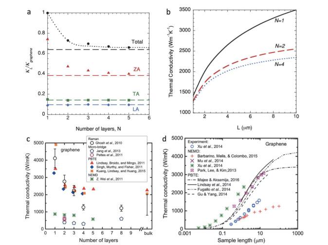
The impact of length and thickness on graphene thermal conductivity 56, 63.
(a) Calculated thermal conductivity for few-layer graphene vs layer number N for N = 1–5 (black circles). Also shown are the per-branch contributions for ZA (red triangles), TA (green squares), and LA (blue diamonds) branches. The corresponding calculated graphite values are shown by the horizontal lines. (b) Calculated thermal conductivity for graphene (N = 1, solid black curve), bilayer graphene (N = 2, dashed red curve), and 4-layer graphene (N = 4, dotted blue curve) as a function of sample length L for T = 300 K. On this scale, the N = 3 and N= 5 curves cannot be distinguished from that for N = 4. Thermal conductivity of graphene as a function of (c) sample length and (d) thickness. Adapted with permission from Ref. 56, Copyright 2011, American Physical Society and Ref. 63, Copyright 2018, American Physical Society.
Fig 3
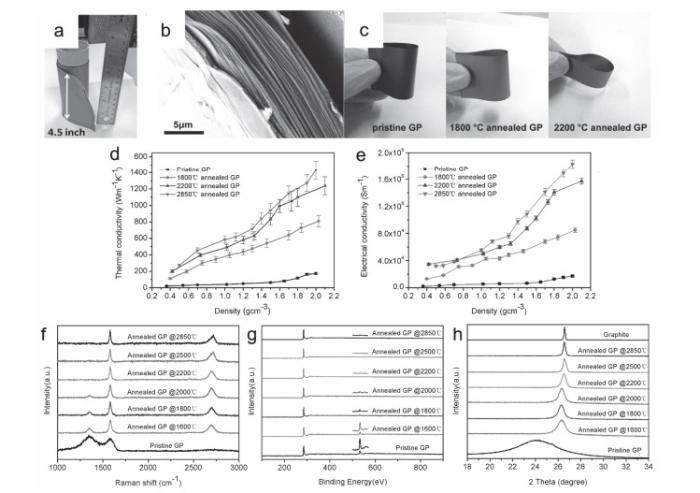
The preparation and characterization of highly thermal conductive graphene film 76.
(a) Graphene film roll with 4.5-inch width (i) made by electrospray deposition integrated with a roll-to-roll process. (b) Cross-sectional SEM image of pristine graphene film made by electrospray deposition showing a layer-by-layer assembly. (f) image of pristine graphene film, graphene film annealed at 1800 ℃ (middle) and 2200 ℃ (right). (d–e) Electrical and thermal properties of freestanding graphene films: (d) Graphene film without thermal annealing and (e) annealed graphene film. The increased density is caused by mechanical press resulting in a more film compact structure. (c–e), Defect recovery, removal of functional groups and improvement of crystallinity of freestanding graphene film by high temperature annealing: (c) Raman spectra, (d) XPS and (e) XRD patterns of the as‐made graphene films and high temperature annealed graphene films. The magnified (by 5 times) O 1s peak has been shown in (d) on the right top of each XPS spectrum. The XRD pattern of pure graphite is included in (e) for comparison. Adapted with permission from Ref. 76, Copyright 2014, John Wiley and Sons.
Fig 4
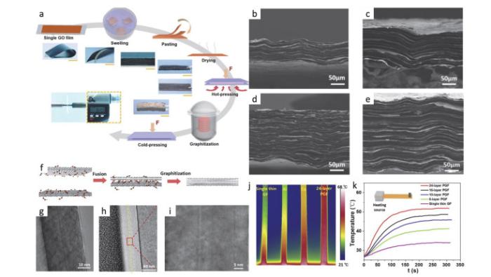
The preparation, characterization and thermal feature of graphene film with a thickness of over 100 μm 81.
(a) Schematic of the fabrication process of the ultrathick GF and photographs at each step. Scale bar from top to bottom: 4, 1, 1, 1, 1, 1 cm. (b–e) A series of thick films pasted with different layers, including 6 layers (b), 12 layers (c), 16 layers (d) and 24 layers (e). (f) Mechanism diagram of the fusion between the two nano-thick films. (g) TEM image of the cross section of an individual 30 nm nano-thick GF. (h, i) TEM images of the pasted 60 nm nano-thick GF, revealing the robust coalescence of the two 30 nm thick films at the contact interface. (j) Infrared thermal image of GFs and metallic foils. The right three samples have a thickness of 200 μm, attached vertically on a constant temperature heat source. (k) Temperature of the graphite bulk versus time when it was heated by 24-layer PGF, 16-layer PGF, 12-layer PGF, 6-layer PGF and single thin PGF. Adapted with permission from Ref. 81, Copyright 2020, Elsevier.
Table 2
表2
表2石墨烯导热膜主要研究成果
Table 2 A summary of study on thermal conductive graphene paper.
Fig 5
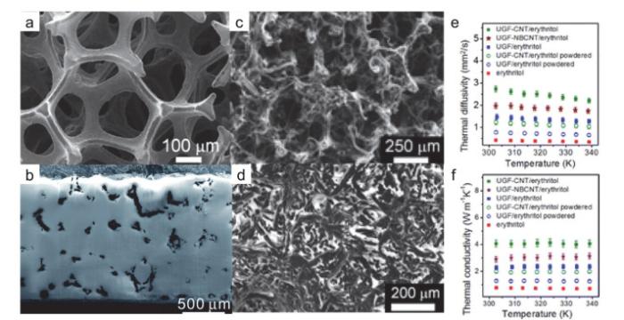
Using graphene foam as 3D thermal conductive network for polymer-based composite 11, 117.
(a) SEM image of UGF before wax filling. (b) SEM of UGF-wax composite. (c) SEM image of UGF-CNT hybrid structure. (d) SEM image of UGF-CNT/erythritol composites. (e) thermal diffusivity, and (f) thermal conductivity of erythritol, UGF/erythritol, and UGF-CNT/erythritol, containing additional data for powdered UGF/erythritol, powdered UGF-CNT/erythritol, and UGF-NBCNT/erythritol composites. Adapted with permission from Refs. 11, 117, Copyright 2014, Royal Society of Chemistry and Ref. 90, Copyright 2015, American Chemical Society.
Scheme of setups for different thermal measurements <sup><xref ref-type="bibr" rid="b49">49</xref></sup>.
(a) Optothermal Raman method. (b) Suspended-pad method. (c) Time-domain thermoreflectance (TDTR) method, where blue and orange lines represent pump and probe laser beams, respectively. (d) Laser flash method, where the left and right parts illustrate measurements of in-plane and cross-plane thermal conductivities. Adapted with permission from Ref. 49, Copyright 2018, Elsevier. ...
Scheme of setups for different thermal measurements <sup><xref ref-type="bibr" rid="b49">49</xref></sup>.
(a) Optothermal Raman method. (b) Suspended-pad method. (c) Time-domain thermoreflectance (TDTR) method, where blue and orange lines represent pump and probe laser beams, respectively. (d) Laser flash method, where the left and right parts illustrate measurements of in-plane and cross-plane thermal conductivities. Adapted with permission from Ref. 49, Copyright 2018, Elsevier. ...
Scheme of setups for different thermal measurements <sup><xref ref-type="bibr" rid="b49">49</xref></sup>.
(a) Optothermal Raman method. (b) Suspended-pad method. (c) Time-domain thermoreflectance (TDTR) method, where blue and orange lines represent pump and probe laser beams, respectively. (d) Laser flash method, where the left and right parts illustrate measurements of in-plane and cross-plane thermal conductivities. Adapted with permission from Ref. 49, Copyright 2018, Elsevier. ...
... 11, 117Using graphene foam as 3D thermal conductive network for polymer-based composite <sup><xref ref-type="bibr" rid="b11">11</xref>, <xref ref-type="bibr" rid="b117">117</xref></sup>.
(a) SEM image of UGF before wax filling. (b) SEM of UGF-wax composite. (c) SEM image of UGF-CNT hybrid structure. (d) SEM image of UGF-CNT/erythritol composites. (e) thermal diffusivity, and (f) thermal conductivity of erythritol, UGF/erythritol, and UGF-CNT/erythritol, containing additional data for powdered UGF/erythritol, powdered UGF-CNT/erythritol, and UGF-NBCNT/erythritol composites. Adapted with permission from Refs. 11, 117, Copyright 2014, Royal Society of Chemistry and Ref. 90, Copyright 2015, American Chemical Society. ...
... 11, 117.
(a) SEM image of UGF before wax filling. (b) SEM of UGF-wax composite. (c) SEM image of UGF-CNT hybrid structure. (d) SEM image of UGF-CNT/erythritol composites. (e) thermal diffusivity, and (f) thermal conductivity of erythritol, UGF/erythritol, and UGF-CNT/erythritol, containing additional data for powdered UGF/erythritol, powdered UGF-CNT/erythritol, and UGF-NBCNT/erythritol composites. Adapted with permission from Refs. 11, 117, Copyright 2014, Royal Society of Chemistry and Ref. 90, Copyright 2015, American Chemical Society. ...
... A summary of highly thermal conductive composite with graphene filler.Table 3
Fillers
Loading
Thermal conductivity/(W·m-1·K-1)
Method
rGO 96
25% (x)
6.4
Mixing
rGO 97
20% (w)
5.8
Silane functionalized
Graphene 98
10% (x)
5.1
Sodium cholate functionalized
rGO 104
5% (w)
1.1
[polyimide] NH2-functionalized, in situ polymerization
Scheme of setups for different thermal measurements <sup><xref ref-type="bibr" rid="b49">49</xref></sup>.
(a) Optothermal Raman method. (b) Suspended-pad method. (c) Time-domain thermoreflectance (TDTR) method, where blue and orange lines represent pump and probe laser beams, respectively. (d) Laser flash method, where the left and right parts illustrate measurements of in-plane and cross-plane thermal conductivities. Adapted with permission from Ref. 49, Copyright 2018, Elsevier. ...
Scheme of setups for different thermal measurements <sup><xref ref-type="bibr" rid="b49">49</xref></sup>.
(a) Optothermal Raman method. (b) Suspended-pad method. (c) Time-domain thermoreflectance (TDTR) method, where blue and orange lines represent pump and probe laser beams, respectively. (d) Laser flash method, where the left and right parts illustrate measurements of in-plane and cross-plane thermal conductivities. Adapted with permission from Ref. 49, Copyright 2018, Elsevier. ...
Scheme of setups for different thermal measurements <sup><xref ref-type="bibr" rid="b49">49</xref></sup>.
(a) Optothermal Raman method. (b) Suspended-pad method. (c) Time-domain thermoreflectance (TDTR) method, where blue and orange lines represent pump and probe laser beams, respectively. (d) Laser flash method, where the left and right parts illustrate measurements of in-plane and cross-plane thermal conductivities. Adapted with permission from Ref. 49, Copyright 2018, Elsevier. ...
Scheme of setups for different thermal measurements <sup><xref ref-type="bibr" rid="b49">49</xref></sup>.
(a) Optothermal Raman method. (b) Suspended-pad method. (c) Time-domain thermoreflectance (TDTR) method, where blue and orange lines represent pump and probe laser beams, respectively. (d) Laser flash method, where the left and right parts illustrate measurements of in-plane and cross-plane thermal conductivities. Adapted with permission from Ref. 49, Copyright 2018, Elsevier. ...
Scheme of setups for different thermal measurements <sup><xref ref-type="bibr" rid="b49">49</xref></sup>.
(a) Optothermal Raman method. (b) Suspended-pad method. (c) Time-domain thermoreflectance (TDTR) method, where blue and orange lines represent pump and probe laser beams, respectively. (d) Laser flash method, where the left and right parts illustrate measurements of in-plane and cross-plane thermal conductivities. Adapted with permission from Ref. 49, Copyright 2018, Elsevier. ...
Scheme of setups for different thermal measurements <sup><xref ref-type="bibr" rid="b49">49</xref></sup>.
(a) Optothermal Raman method. (b) Suspended-pad method. (c) Time-domain thermoreflectance (TDTR) method, where blue and orange lines represent pump and probe laser beams, respectively. (d) Laser flash method, where the left and right parts illustrate measurements of in-plane and cross-plane thermal conductivities. Adapted with permission from Ref. 49, Copyright 2018, Elsevier. ...
Scheme of setups for different thermal measurements <sup><xref ref-type="bibr" rid="b49">49</xref></sup>.
(a) Optothermal Raman method. (b) Suspended-pad method. (c) Time-domain thermoreflectance (TDTR) method, where blue and orange lines represent pump and probe laser beams, respectively. (d) Laser flash method, where the left and right parts illustrate measurements of in-plane and cross-plane thermal conductivities. Adapted with permission from Ref. 49, Copyright 2018, Elsevier. ...
Scheme of setups for different thermal measurements <sup><xref ref-type="bibr" rid="b49">49</xref></sup>.
(a) Optothermal Raman method. (b) Suspended-pad method. (c) Time-domain thermoreflectance (TDTR) method, where blue and orange lines represent pump and probe laser beams, respectively. (d) Laser flash method, where the left and right parts illustrate measurements of in-plane and cross-plane thermal conductivities. Adapted with permission from Ref. 49, Copyright 2018, Elsevier. ...
Scheme of setups for different thermal measurements <sup><xref ref-type="bibr" rid="b49">49</xref></sup>.
(a) Optothermal Raman method. (b) Suspended-pad method. (c) Time-domain thermoreflectance (TDTR) method, where blue and orange lines represent pump and probe laser beams, respectively. (d) Laser flash method, where the left and right parts illustrate measurements of in-plane and cross-plane thermal conductivities. Adapted with permission from Ref. 49, Copyright 2018, Elsevier. ...
Scheme of setups for different thermal measurements <sup><xref ref-type="bibr" rid="b49">49</xref></sup>.
(a) Optothermal Raman method. (b) Suspended-pad method. (c) Time-domain thermoreflectance (TDTR) method, where blue and orange lines represent pump and probe laser beams, respectively. (d) Laser flash method, where the left and right parts illustrate measurements of in-plane and cross-plane thermal conductivities. Adapted with permission from Ref. 49, Copyright 2018, Elsevier. ...
Scheme of setups for different thermal measurements <sup><xref ref-type="bibr" rid="b49">49</xref></sup>.
(a) Optothermal Raman method. (b) Suspended-pad method. (c) Time-domain thermoreflectance (TDTR) method, where blue and orange lines represent pump and probe laser beams, respectively. (d) Laser flash method, where the left and right parts illustrate measurements of in-plane and cross-plane thermal conductivities. Adapted with permission from Ref. 49, Copyright 2018, Elsevier. ...
Scheme of setups for different thermal measurements <sup><xref ref-type="bibr" rid="b49">49</xref></sup>.
(a) Optothermal Raman method. (b) Suspended-pad method. (c) Time-domain thermoreflectance (TDTR) method, where blue and orange lines represent pump and probe laser beams, respectively. (d) Laser flash method, where the left and right parts illustrate measurements of in-plane and cross-plane thermal conductivities. Adapted with permission from Ref. 49, Copyright 2018, Elsevier. ...
... 49.
(a) Optothermal Raman method. (b) Suspended-pad method. (c) Time-domain thermoreflectance (TDTR) method, where blue and orange lines represent pump and probe laser beams, respectively. (d) Laser flash method, where the left and right parts illustrate measurements of in-plane and cross-plane thermal conductivities. Adapted with permission from Ref. 49, Copyright 2018, Elsevier. ...
... (a) Optothermal Raman method. (b) Suspended-pad method. (c) Time-domain thermoreflectance (TDTR) method, where blue and orange lines represent pump and probe laser beams, respectively. (d) Laser flash method, where the left and right parts illustrate measurements of in-plane and cross-plane thermal conductivities. Adapted with permission from Ref. 49, Copyright 2018, Elsevier. ...
The impact of length and thickness on graphene thermal conductivity <sup><xref ref-type="bibr" rid="b56">56</xref>, <xref ref-type="bibr" rid="b63">63</xref></sup>.
(a) Calculated thermal conductivity for few-layer graphene vs layer number N for N = 1–5 (black circles). Also shown are the per-branch contributions for ZA (red triangles), TA (green squares), and LA (blue diamonds) branches. The corresponding calculated graphite values are shown by the horizontal lines. (b) Calculated thermal conductivity for graphene (N = 1, solid black curve), bilayer graphene (N = 2, dashed red curve), and 4-layer graphene (N = 4, dotted blue curve) as a function of sample length L for T = 300 K. On this scale, the N = 3 and N= 5 curves cannot be distinguished from that for N = 4. Thermal conductivity of graphene as a function of (c) sample length and (d) thickness. Adapted with permission from Ref. 56, Copyright 2011, American Physical Society and Ref. 63, Copyright 2018, American Physical Society. ...
... 56, 63.
(a) Calculated thermal conductivity for few-layer graphene vs layer number N for N = 1–5 (black circles). Also shown are the per-branch contributions for ZA (red triangles), TA (green squares), and LA (blue diamonds) branches. The corresponding calculated graphite values are shown by the horizontal lines. (b) Calculated thermal conductivity for graphene (N = 1, solid black curve), bilayer graphene (N = 2, dashed red curve), and 4-layer graphene (N = 4, dotted blue curve) as a function of sample length L for T = 300 K. On this scale, the N = 3 and N= 5 curves cannot be distinguished from that for N = 4. Thermal conductivity of graphene as a function of (c) sample length and (d) thickness. Adapted with permission from Ref. 56, Copyright 2011, American Physical Society and Ref. 63, Copyright 2018, American Physical Society. ...
... (a) Calculated thermal conductivity for few-layer graphene vs layer number N for N = 1–5 (black circles). Also shown are the per-branch contributions for ZA (red triangles), TA (green squares), and LA (blue diamonds) branches. The corresponding calculated graphite values are shown by the horizontal lines. (b) Calculated thermal conductivity for graphene (N = 1, solid black curve), bilayer graphene (N = 2, dashed red curve), and 4-layer graphene (N = 4, dotted blue curve) as a function of sample length L for T = 300 K. On this scale, the N = 3 and N= 5 curves cannot be distinguished from that for N = 4. Thermal conductivity of graphene as a function of (c) sample length and (d) thickness. Adapted with permission from Ref. 56, Copyright 2011, American Physical Society and Ref. 63, Copyright 2018, American Physical Society. ...
The impact of length and thickness on graphene thermal conductivity <sup><xref ref-type="bibr" rid="b56">56</xref>, <xref ref-type="bibr" rid="b63">63</xref></sup>.
(a) Calculated thermal conductivity for few-layer graphene vs layer number N for N = 1–5 (black circles). Also shown are the per-branch contributions for ZA (red triangles), TA (green squares), and LA (blue diamonds) branches. The corresponding calculated graphite values are shown by the horizontal lines. (b) Calculated thermal conductivity for graphene (N = 1, solid black curve), bilayer graphene (N = 2, dashed red curve), and 4-layer graphene (N = 4, dotted blue curve) as a function of sample length L for T = 300 K. On this scale, the N = 3 and N= 5 curves cannot be distinguished from that for N = 4. Thermal conductivity of graphene as a function of (c) sample length and (d) thickness. Adapted with permission from Ref. 56, Copyright 2011, American Physical Society and Ref. 63, Copyright 2018, American Physical Society. ...
... , 63.
(a) Calculated thermal conductivity for few-layer graphene vs layer number N for N = 1–5 (black circles). Also shown are the per-branch contributions for ZA (red triangles), TA (green squares), and LA (blue diamonds) branches. The corresponding calculated graphite values are shown by the horizontal lines. (b) Calculated thermal conductivity for graphene (N = 1, solid black curve), bilayer graphene (N = 2, dashed red curve), and 4-layer graphene (N = 4, dotted blue curve) as a function of sample length L for T = 300 K. On this scale, the N = 3 and N= 5 curves cannot be distinguished from that for N = 4. Thermal conductivity of graphene as a function of (c) sample length and (d) thickness. Adapted with permission from Ref. 56, Copyright 2011, American Physical Society and Ref. 63, Copyright 2018, American Physical Society. ...
... (a) Calculated thermal conductivity for few-layer graphene vs layer number N for N = 1–5 (black circles). Also shown are the per-branch contributions for ZA (red triangles), TA (green squares), and LA (blue diamonds) branches. The corresponding calculated graphite values are shown by the horizontal lines. (b) Calculated thermal conductivity for graphene (N = 1, solid black curve), bilayer graphene (N = 2, dashed red curve), and 4-layer graphene (N = 4, dotted blue curve) as a function of sample length L for T = 300 K. On this scale, the N = 3 and N= 5 curves cannot be distinguished from that for N = 4. Thermal conductivity of graphene as a function of (c) sample length and (d) thickness. Adapted with permission from Ref. 56, Copyright 2011, American Physical Society and Ref. 63, Copyright 2018, American Physical Society. ...
... 76The preparation and characterization of highly thermal conductive graphene film <sup><xref ref-type="bibr" rid="b76">76</xref></sup>.
(a) Graphene film roll with 4.5-inch width (i) made by electrospray deposition integrated with a roll-to-roll process. (b) Cross-sectional SEM image of pristine graphene film made by electrospray deposition showing a layer-by-layer assembly. (f) image of pristine graphene film, graphene film annealed at 1800 ℃ (middle) and 2200 ℃ (right). (d–e) Electrical and thermal properties of freestanding graphene films: (d) Graphene film without thermal annealing and (e) annealed graphene film. The increased density is caused by mechanical press resulting in a more film compact structure. (c–e), Defect recovery, removal of functional groups and improvement of crystallinity of freestanding graphene film by high temperature annealing: (c) Raman spectra, (d) XPS and (e) XRD patterns of the as‐made graphene films and high temperature annealed graphene films. The magnified (by 5 times) O 1s peak has been shown in (d) on the right top of each XPS spectrum. The XRD pattern of pure graphite is included in (e) for comparison. Adapted with permission from Ref. 76, Copyright 2014, John Wiley and Sons. ...
... 76.
(a) Graphene film roll with 4.5-inch width (i) made by electrospray deposition integrated with a roll-to-roll process. (b) Cross-sectional SEM image of pristine graphene film made by electrospray deposition showing a layer-by-layer assembly. (f) image of pristine graphene film, graphene film annealed at 1800 ℃ (middle) and 2200 ℃ (right). (d–e) Electrical and thermal properties of freestanding graphene films: (d) Graphene film without thermal annealing and (e) annealed graphene film. The increased density is caused by mechanical press resulting in a more film compact structure. (c–e), Defect recovery, removal of functional groups and improvement of crystallinity of freestanding graphene film by high temperature annealing: (c) Raman spectra, (d) XPS and (e) XRD patterns of the as‐made graphene films and high temperature annealed graphene films. The magnified (by 5 times) O 1s peak has been shown in (d) on the right top of each XPS spectrum. The XRD pattern of pure graphite is included in (e) for comparison. Adapted with permission from Ref. 76, Copyright 2014, John Wiley and Sons. ...
... (a) Graphene film roll with 4.5-inch width (i) made by electrospray deposition integrated with a roll-to-roll process. (b) Cross-sectional SEM image of pristine graphene film made by electrospray deposition showing a layer-by-layer assembly. (f) image of pristine graphene film, graphene film annealed at 1800 ℃ (middle) and 2200 ℃ (right). (d–e) Electrical and thermal properties of freestanding graphene films: (d) Graphene film without thermal annealing and (e) annealed graphene film. The increased density is caused by mechanical press resulting in a more film compact structure. (c–e), Defect recovery, removal of functional groups and improvement of crystallinity of freestanding graphene film by high temperature annealing: (c) Raman spectra, (d) XPS and (e) XRD patterns of the as‐made graphene films and high temperature annealed graphene films. The magnified (by 5 times) O 1s peak has been shown in (d) on the right top of each XPS spectrum. The XRD pattern of pure graphite is included in (e) for comparison. Adapted with permission from Ref. 76, Copyright 2014, John Wiley and Sons. ...
... A summary of study on thermal conductive graphene paper.Table 2
Material
Thermal conductivity/(W·m-1·K-1)
Preparation method
GO 9
2025
Doctor-blade, 3000 ℃ annealing reduction +3000 ℃ second annealing reduction
... 81The preparation, characterization and thermal feature of graphene film with a thickness of over 100 μm <sup><xref ref-type="bibr" rid="b81">81</xref></sup>.
(a) Schematic of the fabrication process of the ultrathick GF and photographs at each step. Scale bar from top to bottom: 4, 1, 1, 1, 1, 1 cm. (b–e) A series of thick films pasted with different layers, including 6 layers (b), 12 layers (c), 16 layers (d) and 24 layers (e). (f) Mechanism diagram of the fusion between the two nano-thick films. (g) TEM image of the cross section of an individual 30 nm nano-thick GF. (h, i) TEM images of the pasted 60 nm nano-thick GF, revealing the robust coalescence of the two 30 nm thick films at the contact interface. (j) Infrared thermal image of GFs and metallic foils. The right three samples have a thickness of 200 μm, attached vertically on a constant temperature heat source. (k) Temperature of the graphite bulk versus time when it was heated by 24-layer PGF, 16-layer PGF, 12-layer PGF, 6-layer PGF and single thin PGF. Adapted with permission from Ref. 81, Copyright 2020, Elsevier. ...
... 81.
(a) Schematic of the fabrication process of the ultrathick GF and photographs at each step. Scale bar from top to bottom: 4, 1, 1, 1, 1, 1 cm. (b–e) A series of thick films pasted with different layers, including 6 layers (b), 12 layers (c), 16 layers (d) and 24 layers (e). (f) Mechanism diagram of the fusion between the two nano-thick films. (g) TEM image of the cross section of an individual 30 nm nano-thick GF. (h, i) TEM images of the pasted 60 nm nano-thick GF, revealing the robust coalescence of the two 30 nm thick films at the contact interface. (j) Infrared thermal image of GFs and metallic foils. The right three samples have a thickness of 200 μm, attached vertically on a constant temperature heat source. (k) Temperature of the graphite bulk versus time when it was heated by 24-layer PGF, 16-layer PGF, 12-layer PGF, 6-layer PGF and single thin PGF. Adapted with permission from Ref. 81, Copyright 2020, Elsevier. ...
... (a) Schematic of the fabrication process of the ultrathick GF and photographs at each step. Scale bar from top to bottom: 4, 1, 1, 1, 1, 1 cm. (b–e) A series of thick films pasted with different layers, including 6 layers (b), 12 layers (c), 16 layers (d) and 24 layers (e). (f) Mechanism diagram of the fusion between the two nano-thick films. (g) TEM image of the cross section of an individual 30 nm nano-thick GF. (h, i) TEM images of the pasted 60 nm nano-thick GF, revealing the robust coalescence of the two 30 nm thick films at the contact interface. (j) Infrared thermal image of GFs and metallic foils. The right three samples have a thickness of 200 μm, attached vertically on a constant temperature heat source. (k) Temperature of the graphite bulk versus time when it was heated by 24-layer PGF, 16-layer PGF, 12-layer PGF, 6-layer PGF and single thin PGF. Adapted with permission from Ref. 81, Copyright 2020, Elsevier. ...
... A summary of study on thermal conductive graphene paper.Table 2
Material
Thermal conductivity/(W·m-1·K-1)
Preparation method
GO 9
2025
Doctor-blade, 3000 ℃ annealing reduction +3000 ℃ second annealing reduction
... (a) SEM image of UGF before wax filling. (b) SEM of UGF-wax composite. (c) SEM image of UGF-CNT hybrid structure. (d) SEM image of UGF-CNT/erythritol composites. (e) thermal diffusivity, and (f) thermal conductivity of erythritol, UGF/erythritol, and UGF-CNT/erythritol, containing additional data for powdered UGF/erythritol, powdered UGF-CNT/erythritol, and UGF-NBCNT/erythritol composites. Adapted with permission from Refs. 11, 117, Copyright 2014, Royal Society of Chemistry and Ref. 90, Copyright 2015, American Chemical Society. ...
... , 117Using graphene foam as 3D thermal conductive network for polymer-based composite <sup><xref ref-type="bibr" rid="b11">11</xref>, <xref ref-type="bibr" rid="b117">117</xref></sup>.
(a) SEM image of UGF before wax filling. (b) SEM of UGF-wax composite. (c) SEM image of UGF-CNT hybrid structure. (d) SEM image of UGF-CNT/erythritol composites. (e) thermal diffusivity, and (f) thermal conductivity of erythritol, UGF/erythritol, and UGF-CNT/erythritol, containing additional data for powdered UGF/erythritol, powdered UGF-CNT/erythritol, and UGF-NBCNT/erythritol composites. Adapted with permission from Refs. 11, 117, Copyright 2014, Royal Society of Chemistry and Ref. 90, Copyright 2015, American Chemical Society. ...
... , 117.
(a) SEM image of UGF before wax filling. (b) SEM of UGF-wax composite. (c) SEM image of UGF-CNT hybrid structure. (d) SEM image of UGF-CNT/erythritol composites. (e) thermal diffusivity, and (f) thermal conductivity of erythritol, UGF/erythritol, and UGF-CNT/erythritol, containing additional data for powdered UGF/erythritol, powdered UGF-CNT/erythritol, and UGF-NBCNT/erythritol composites. Adapted with permission from Refs. 11, 117, Copyright 2014, Royal Society of Chemistry and Ref. 90, Copyright 2015, American Chemical Society. ...
... A summary of highly thermal conductive composite with graphene filler.Table 3
Fillers
Loading
Thermal conductivity/(W·m-1·K-1)
Method
rGO 96
25% (x)
6.4
Mixing
rGO 97
20% (w)
5.8
Silane functionalized
Graphene 98
10% (x)
5.1
Sodium cholate functionalized
rGO 104
5% (w)
1.1
[polyimide] NH2-functionalized, in situ polymerization