Acta Phys. -Chim. Sin. ›› 2025, Vol. 41 ›› Issue (4): 100030.doi: 10.3866/PKU.WHXB202309045
Special Issue: Next-Generation Optoelectronic Functional Materials
• REVIEW • Previous Articles Next Articles
Progress and Perspective of Perovskite Thin Single Crystal Photodetectors
Yao Ma, Xin Zhao, Hongxu Chen, Wei Wei, Liang Shen*( )
)
- International Center of Future Science, State Key Laboratory of Integrated Optoelectronics, College of Electronic Science and Engineering, Jilin University, Changchun 130012, China
-
Received:2023-09-28Revised:2023-11-04Accepted:2023-11-06Published:2023-12-20 -
Contact:Email: shenliang@jlu.edu.cn; Tel.: +86-431-85168241 (Liang Shen) -
Supported by:the International Cooperation and Exchange Project of Jilin Province(20210402079GH); the International Cooperation and Exchange Project of Jilin Province(20230402056GH); the 19th Batch of Innovative and Entrepreneurial Talent Projects in Jilin Province(2023QN01); the Project of Science and Technology Development Plan of Jilin Province(20220508037RC); the Graduate Innovation Fund of Jilin University

Cite this article
Yao Ma, Xin Zhao, Hongxu Chen, Wei Wei, Liang Shen. Progress and Perspective of Perovskite Thin Single Crystal Photodetectors[J]. Acta Phys. -Chim. Sin. 2025, 41(4), 100030. doi: 10.3866/PKU.WHXB202309045
share this article
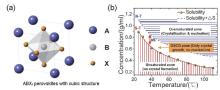
Fig 1
(a) Depiction of ABX3 perovskites with cubic structure 22; (b) Solubility curve and concentration vs. the growth temperature for different regions in the single-crystal growth model 29. (a) Adapted from Royal Society of Chemistry publlisher; (b) Adapted from Elsevier publisher."
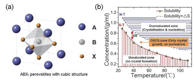
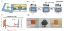
Fig 2
(a) The growth mechanism of (FAPbI3)0.85(MAPbBr3)0.15 single crystals by the PDMS-assisted solvent evaporation crystallization method photographs 31; (b) Schematic diagram of controlling solvent volatilization through a valve 33; (c) Growth mechanism diagram 33; (d) Photograph of MAPbBr3, MAPbI3, and CsPbBr3 single crystal grown by solvent evaporation method 33. (a) Adapted from John Wiley and Sons publisher; (b–d) Adapted from Elsevier publisher."
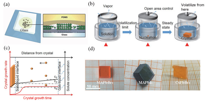
Fig 3
(a) Schematic diagram of the crystallization process 35; (b) Left: MAPbBr3, Right: MAPbI3 35; Illustration: band gap determined by absorbance and photonenergy; (c) Schematic diagram of the Anti-solvent vapor-assisted capping crystallization process 36; (d) Mechanism diagram at micro scale 37. (a, b) Adapted from The American Association for the Advancement of Science publisher; (c) Adapted from Royal Society of Chemistry publisher; (d) Adapted from John Wiley and Sons publisher."
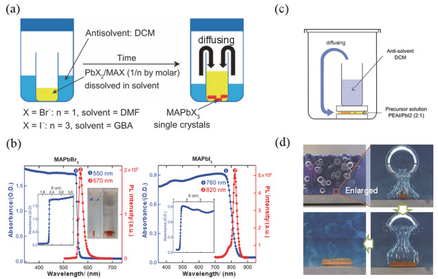
Fig 4
(a) The set up for large MAPbI3 single crystals growth 39; (b) Images of a piece of as-prepared MAPbI3 single crystal 39; (c) Schematic experimental observation 40; (d) Photograph of freshly grown crystals 40, 1 blue square = 1 mm2; (e) MAPbBr3 crystal growth at different time intervals 41. (a, b) Adapted from The American Association for the Advancement of Science publisher; (c–e) Adapted from Springer Nature publisher."
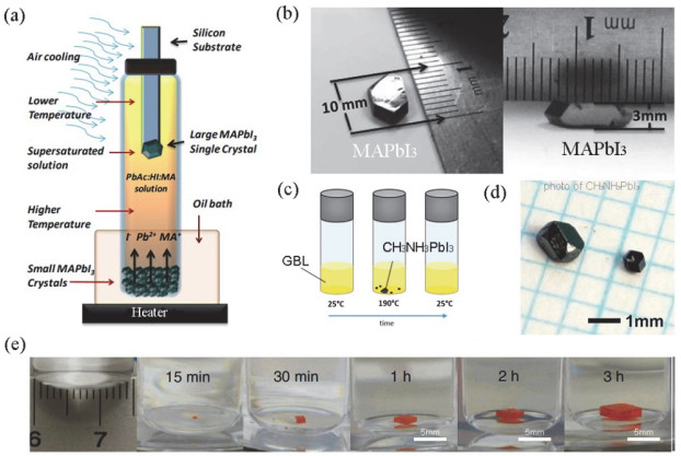
Fig 5
(a) A schematic illustration for the ultrathin single crystal wafer preparation 42; (b) Photo of an single crystal wafer growing in the microreactor system 42; (c) Schematic representation of the procedure for fabricating planar MAPbI3 single crystals of micrometer-scale thickness 43; (d) XRD spectrum of an single crystal plate 43. (a–d) Adapted from John Wiley and Sons publisher."
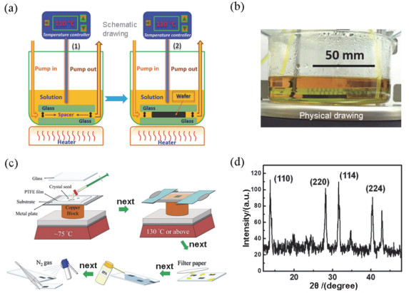
Fig 6
(a) Schematic of cast-capping method 44; (b) Schematic diagram of the module to grow laminar MAPbBr3 crystal films 45, whose thickness was defined by polytetrafluoroethylene (PTFE) thin membranes' thickness; (c) Photographs of the diffusion process of methylammonium lead triiodide precursor solution in the confined gaps after different durations using hydrophilic glass and hydrophobic PTAA-covered ITO substrates 46; (d) Scheme for growth of perovskite single-crystalline thin films 47; (e) Optical images of ultrathin MAPbBr3 single crystal films showing the thickness-dependent colors 47. (a) Adapted from Elsevier publisher; (b) Adapted from John Wiley and Sons publisher; (c) Adapted from Springer Nature publisher; (d, e) Adapted from American Chemical Society publisher"
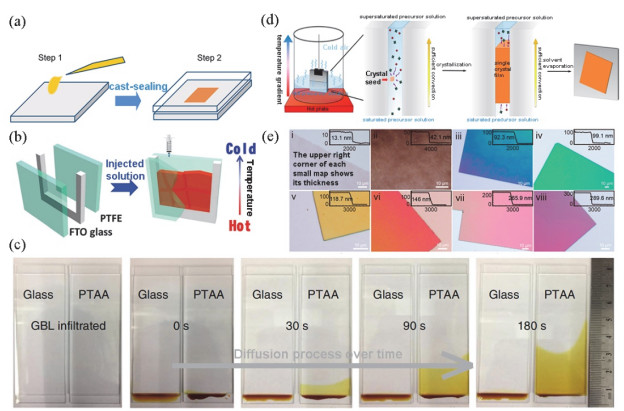
Fig 7
(a) Schematic of crystal growth during inversion crystallization 48; Photographs of (b) free-standing MAPbBr3 and (c) MAPbBr3, (d) MAPbI3, and (e) MASnBr3 perovskite single crystal films floating on the solution surfaces 48; (f) Schematic of surface tension-controlled crystallization process 49. (g) Photographs of the (PEA)2PbI4 perovskite single crystal grown at different temperatures 49; (h) XRD patterns of a 2D (PEA)2PbI4 perovskite single crystal recorded from (001) and (010) planes 49. (a–e) Adapted from American Chemical Society publisher; (f–h) Adapted from Elsevier publisher."
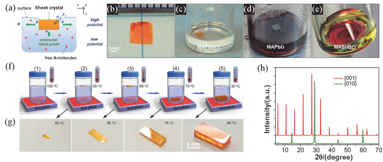
Fig 8
(a) Plot of lattice constants versus band gap for the halide perovskite family including both hybrid (red legends), pure inorganic (blue legends), and Sn (green legends) based perovskites, which covers the entire visible light range 50; (b) Illustration of the incommensurate lattice match between CsPbBr3(100) and STO(100) crystallographic planes 51; (c) Cross-sectional SEM images and photographs of the CsPbBr3 single crystal films with varying thickness of 1, 2, 5, and 7 μm 51; (d) The schematic illustration of the wafer slicing process 52; (e) A schematic illustration for the preparation of a MAPbI3 single crystalline film by the top-down method 53; (f) The X-ray rocking curves for the (400) plane of a MAPbI3 single crystal before and after thinning 53. (a) Adapted from John Wiley and Sons publisher; (b–d) Adapted from Springer Nature publisher; (e, f) Adapted from Royal Society of Chemistry publisher."
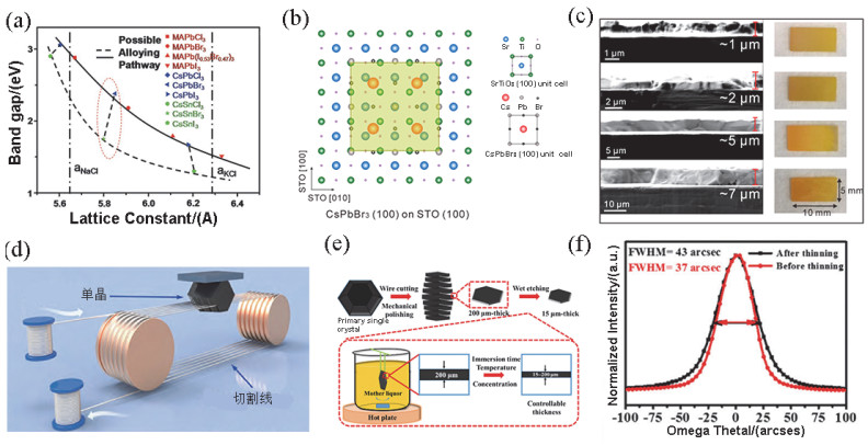
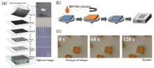
Fig 9
(a) Schematics (left) and corresponding optical images (right) showing the solution-based epitaxial growth, merging and transferring processes of the single-crystal perovskite thin film 54; (b) Schematic diagram of the MAPbBr3 microdisk preparation process 55; (c) Microscopic images of perovskite crystals changing from octagon to square 55. (a) Adapted from Springer Nature publisher; (b, c) Adapted from Royal Society of Chemistry publisher."
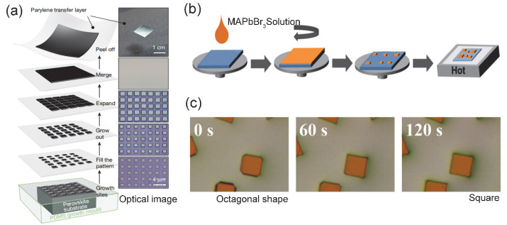
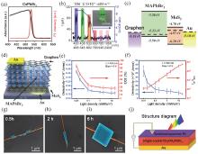
Fig 10
(a) The UV-Vis absorption spectrum (in black) and the PL spectrum(in red) of CsPbBr3 crystal for comparison (black lines) 18; (b) The photo response (dark line)and on/off ratio (blue line)of the CsPbBr3 vacuum nano-photodiode at 10 Ⅴ under the illumination of light with different wavelengths at a power density of 3.1 × 10⁻⁴ mW∙m−2. The schematic showing the CsPbBr3 vacuum nano-photodiodes under the light illumination is shown in the inset 18; (c) Band diagram of few-layer graphene, MAPbBr3 single crystal thin film, MoS2 flake, and Au before contact 56; (d) Diagram of the MAPbBr3/MoS2 vertical heterostructure device. From the top to the bottom are Au electrode, few-layer graphene, MAPbBr3 single crystal thin film, MoS2 flake, and Au electrode 56; (e) Responsivity and external quantum efficiency as a function of light illumination power density at bias @ 0 Ⅴ for 532 nm 56. (f) Detectivity and Iph/Idark as a function of light illumination power density at bias @ 0 Ⅴ for 532 nm 56. (g–i) False color SEM images of the intermediates obtained at (g) 0.5 h, (h) 2 h, (i) 6 h. Thickness of perovskite: 0.5 µm 57; (j) Schematic structure of the single-crystal perovskite photodetector 58. (a, b) Adapted from MDPI AG publisher; (c–f) Adapted from John Wiley and Sons publisher; (g–i) Adapted from Elsevier publisher; (j) Adapted from Royal Society of Chemistry publisher."
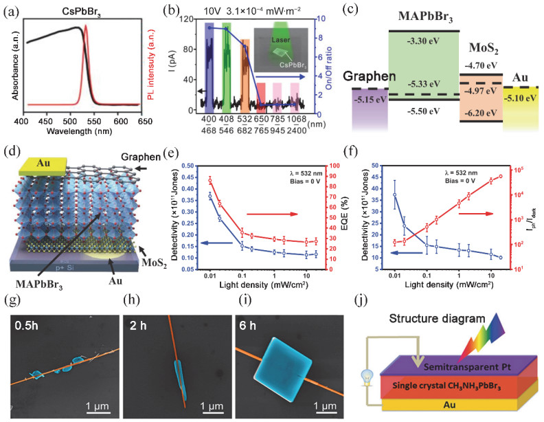
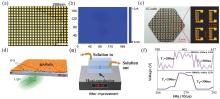
Fig 11
(a) Optical image of electrode arrays on the perovskite single-crystal film 59. Scale bar, 200 mm; (b) Photocurrent mapping of the perovskite single-crystal film 59; (c) Photograph of ~100 photodetectors fabricated on an SC wafer 42, with each sensor consisting of a pair of interdigitated gold (Au) wire electrodes, each of which made of a group of four thin Au wires (1 mm in length, 40 µm in width, and ~300 nm in thickness). The effective illumination area of each detector is 0.12 mm2; (d) Three-dimensional illustration of the photodetector: the MAPbBr3 perovskite layer (orange) is deposited on top of the ITO contacts (light blue). The detector lay on a glass substrate (transparent grey) 61; (e) Schematic diagram of the improved confined space inverse temperature crystallization 62; (f) The enlarged V–t curve to estimate the rise and decay time 62. (a–f) Adapted from John Wiley and Sons publisher."
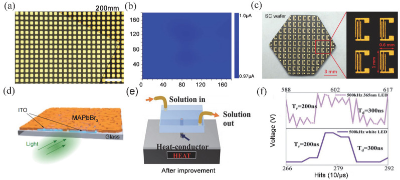
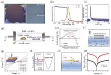
Fig 12
(a) Digital photo of patterned growth on a 2 inch silicon wafer 63. The scale bar is 100 μm. (b) UV-Vis absorption and photoluminescence spectra of the MAPbBr3 microplate array 63. (c) PL decay trace of the MAPbBr3 microplate array 63. (d) Schematic diagram of the tube furnace setup for the growth of CsPbBr3/PbS heterostructures 64. (e) Current–voltage (I–V) curves of the film photodetector in the dark and under 450 nm laser illumination with different light intensities. The inset is the schematic diagram of the device 64. (f) Simplified schematic diagram of precursor ion distribution at the gas-liquid interface 65. (g) Comparison of nucleation barriers between the solution surface and volume 65. (h) Diagram illustrating the energy changes for the growth of a crystal from precursor molecules 65. (i) Schematic of the BA2PbBr4 single crystal films floating on the solution surface 65. (j) I–V curves of the UV photodetectors in the dark and under AM 1.5 illumination 65. (a–c) Adapted from John Wiley and Sons publisher; (d, e) Adapted from IOP Publishing Ltd. publisher; (f–j) Adapted from Royal Society of Chemistry publisher."
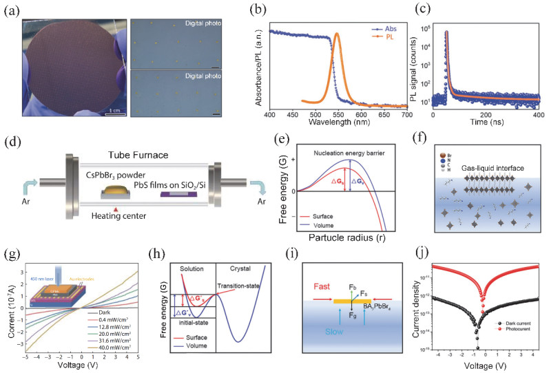
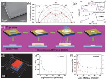
Fig 13
(a) Clear and sharp edges of nanopatterned sample 66; (b) Polarization dependence of normalized photocurrent at 1.11 Ⅴ 66; (c) Schematic illustration of the growth of single-crystal perovskite sheets by dimethicone/MAPbCl3-DMSO biphasic liquid-liquid films 19; (d) 3D pseudo color plot of MAPbBr3 single crystal thickness, the thickness is 2.25 μm 67; (e) Gain 67, and (f) responsivity and detectivity as a function of incident light intensity 67. (a, b) Adapted from John Wiley and Sons publisher; (c) Adapted from American Chemical Society publisher; (d–f) Adapted from John Wiley and Sons publisher."
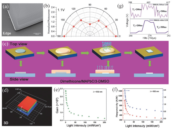
Fig 14
(a) Photograph of electrode arrays on the CsPbCl3 single crystal films 68. Inset shows the partial corresponding optical microscopy image. (b) Temporal photoresponse curves of the device at 293, 343, 203 K and after heated up to 293 K 68. All of the temperature-changing processes were manipulated in about 20 min. (c) Ids–Vds curves of the device measured in dark and light 68. Here, the applied laser is 375 nm with plight ranging from 4.4 μW∙cm−2 to 27.9 W∙cm−2; (d) Normalized Ids of the devices running time at changed temperature in the order from 293 to 343 K and then to 203 K 68. (a–d) Adapted from John Wiley and Sons publisher."
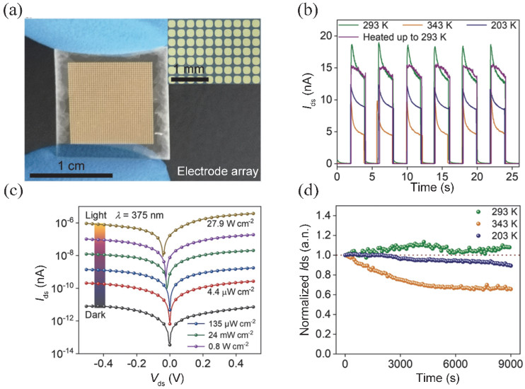
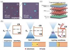
Fig 15
(a) OM images of MAPbBr3 platelets on graphene with different scales 69. (b) Energy band diagrams of graphene and MAPbBr3 platelets before contact, under dark and light conditions, respectively 69. (c) Schematic diagram of the phototransistor memory with perovskite PNC as nano-floating-gates 20. (a–c) Adapted from John Wiley and Sons publisher."
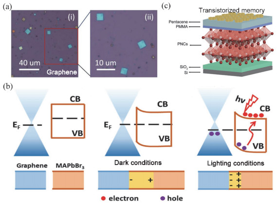

Table 1
Single crystal obtained by different single crystal growth methods."
| Growth method | Single crystal name | Lateral size | Vertical size | Ref. |
| Space-confined method | MAPbBr3 | Area 120 cm2 | 0.1–0.8 mm | |
| Space-confined method | MAPbBr3/MAPbI3 | – | 10–40 μm | |
| Space-confined method | MAPbX3 | Submillimeter-level | From nanometer to micron | |
| Surface tension controlled | MABX3 (B = Pb/Sn, X = Br/I) | 1 cm2 | 5–10 μm | |
| Surface tension controlled | (PEA)2PbI4 | Length 36 mm | – | |
| Vapor phase epitaxy | CsPbBr3/CsSnBr3 | centimeter-level | From nanometer to micron | |
| Vapor phase epitaxy | CsPbBr3 | 10 mm × 5 mm | 1–7 μm | |
| Top-down | MAPbX3 | – | 15–200 μm | |
| Lithography-assisted epitaxial | MAPbI3 | 5.5 cm × 5.5 cm | 0.6–100 μm | |
| Spin coating | MAPbBr3 | Length 3 μm–13 μm | – |
Table 2
Device type and performance parameters."
| Device type | Growth method | Structure | Responsivity | Specific detectivity | Ref. |
| Photodiode | Chemical vapor deposition | Si/CsPbBr3 | 1.75 A∙W−1 | 1.41 × 10¹¹ Jones | |
| Photodiode | Space-confined method | Au/MoS2/MAPbBr3/Gt/Au | 368 mA∙W−1 | 3.74 × 10¹² Jones | |
| Photodiode | Anti-solvent method | CsPbBr3/ZnO | 3.5 × 10³ A∙W−1 | 6.6 × 10¹³ Jones | |
| Photodiode | Anti-solvent method | Pt/MAPbBr3 | ~4.5 mA∙W−1 | 7.1 × 10¹¹ Jones | |
| Photoconductor | Space-confined method | Si/Cs3Bi2I9 | ~3 mA∙W−1 | ~3 × 10¹¹ Jones | |
| Photoconductor | Crystal merge | ITO/MAPbBr3 | 4000 A∙W−1 | > 1013 Jones | |
| Photoconductor | Vapor phase epitaxy | CsPbBr3/PbS | 15 A∙W−1 | 2.65 × 10¹¹ Jones | |
| Photoconductor | Space-confined method | Au/BA2PbBr4/Au | ~45 mA∙W−1 | ~1012 Jones | |
| Photoconductor | Space-confined method | Graphene/MAPbBr3 | ~1017.1 A∙W−1 | ~2.02 × 10¹³ Jones | |
| Photoconductor | Vapor phase epitaxy | CsPbI3/Au | 32.8 A∙W−1 | 4.22 × 10¹² Jones |
| 1 |
doi: 10.1039/c3ee43161d |
| 2 |
doi: 10.1002/adma.201306281 |
| 3 |
doi: 10.1039/c5cp00448a |
| 4 |
doi: 10.1038/ncomms4586 |
| 5 |
doi: 10.1038/nphys3357 |
| 6 |
doi: 10.1038/nphoton.2015.156 |
| 7 |
doi: 10.1038/s41467-019-08768-z |
| 8 |
doi: 10.1002/smll.201903599 |
| 9 |
doi: 10.1021/acs.nanolett.1c00700 |
| 10 |
doi: 10.1002/smll.202001534 |
| 11 |
doi: 10.1126/science.abp8873 |
| 12 |
doi: 10.1038/s41586-023-06514-6 |
| 13 |
doi: 10.1038/s41377-020-0264-5 |
| 14 |
doi: 10.1038/s41566-022-01024-9 |
| 15 |
|
|
卢岳; 葛杨; 隋曼龄. 物理化学学报., 2022, 38 (5), 2007088.
doi: 10.3866/PKU.WHXB202007088 |
|
| 16 |
|
|
杨帅; 徐瑜歆; 郝子坤; 秦胜建; 张润鹏; 韩钰; 杜利伟; 朱紫洢; 杜安宁; 陈欣; 等. 物理化学学报., 2023, 39 (5), 2211025.
doi: 10.3866/PKU.WHXB202211025 |
|
| 17 |
|
|
张涛; 龚思敏; 陈平; 陈琪; 陈立桅. 物理化学学报, 2023, 39 (12), 2301024.
doi: 10.3866/PKU.WHXB202301024 |
|
| 18 |
doi: 10.3390/nano12234205 |
| 19 |
doi: 10.1021/acs.jpclett.1c02905 |
| 20 |
doi: 10.1002/adma.202208497 |
| 21 |
doi: 10.1002/adma.202205261 |
| 22 |
doi: 10.1039/c8cs00740c |
| 23 |
doi: 10.1039/c4mh00174e |
| 24 |
doi: 10.1002/adma.201502597 |
| 25 |
doi: 10.1002/anie.201511792 |
| 26 |
doi: 10.1039/c5cc06916e |
| 27 |
doi: 10.1038/s41467-017-00567-8 |
| 28 |
doi: 10.1038/s41467-021-21805-0 |
| 29 |
doi: 10.1016/j.mattod.2018.04.002 |
| 30 |
doi: 10.1038/ncomms8338 |
| 31 |
doi: 10.1002/admi.201800224 |
| 32 |
doi: 10.1039/c8ce01939h |
| 33 |
doi: 10.1016/j.scib.2021.06.016 |
| 34 |
doi: 10.1038/nmat4014 |
| 35 |
doi: 10.1126/science.aaa2725 |
| 36 |
doi: 10.1039/c7ce00240h |
| 37 |
doi: 10.1002/adma.201506292 |
| 38 |
doi: 10.1039/c4ce02106a |
| 39 |
doi: 10.1126/science.aaa5760 |
| 40 |
doi: 10.1038/srep11654 |
| 41 |
doi: 10.1038/ncomms8586 |
| 42 |
doi: 10.1002/adma.201601995 |
| 43 |
doi: 10.1002/aelm.201700655 |
| 44 |
doi: 10.1016/j.jcrysgro.2016.11.034 |
| 45 |
doi: 10.1002/adma.201602639 |
| 46 |
doi: 10.1038/s41467-017-02039-5 |
| 47 |
doi: 10.1021/jacs.6b09388 |
| 48 |
doi: 10.1021/acsenergylett.7b00468 |
| 49 |
doi: 10.1016/j.matt.2019.04.002 |
| 50 |
doi: 10.1002/adma.201702643 |
| 51 |
doi: 10.1021/jacs.7b07506 |
| 52 |
doi: 10.1007/s11426-017-9081-3 |
| 53 |
doi: 10.1039/c8tc00842f |
| 54 |
doi: 10.1038/s41586-020-2526-z |
| 55 |
doi: 10.1039/d2tc05392f |
| 56 |
doi: 10.1002/admi.202200912 |
| 57 |
doi: 10.1016/j.nantod.2020.101055 |
| 58 |
doi: 10.1039/c6tc02828d |
| 59 |
doi: 10.1126/sciadv.aat2390 |
| 60 |
doi: 10.1002/adma.202103010 |
| 61 |
doi: 10.1038/ncomms9724 |
| 62 |
doi: 10.1002/smll.202203565 |
| 63 |
doi: 10.1002/adfm.202209563 |
| 64 |
doi: 10.1088/1674-4926/42/11/112001 |
| 65 |
doi: 10.1039/d1tc00408e |
| 66 |
doi: 10.1002/adom.202100524 |
| 67 |
doi: 10.1002/smll.202000733 |
| 68 |
doi: 10.1002/adfm.202213360 |
| 69 |
doi: 10.1002/adfm.201909672 |
| 70 |
doi: 10.1016/j.scib.2017.08.022 |
| 71 |
doi: 10.1002/adfm.201905021 |
| 72 |
|
|
陈亮; 田中群. 物理化学学报, 2021, 37 (3), 2010065.
doi: 10.3866/PKU.WHXB202010065 |
|
| 73 |
doi: 10.1038/s41467-018-07177-y |
| 74 |
doi: 10.1038/s41566-023-01167-3 |
| 75 |
doi: 10.1126/sciadv.abc8844 |
| 76 |
doi: 10.1002/adma.202001998 |
| 77 |
doi: 10.1126/science.aba0893 |
| [1] | Binbin Liu, Yang Chen, Tianci Jia, Chen Chen, Zhanghao Wu, Yuhui Liu, Yuhang Zhai, Tianshu Ma, Changlei Wang. Hydroxyl-functionalized molecular engineering mitigates 2D phase barriers for efficient wide-bandgap and all-perovskite tandem solar cells [J]. Acta Phys. -Chim. Sin., 2026, 42(1): 100128-. |
| [2] | Ying Liang, Yuheng Deng, Shilv Yu, Jiahao Cheng, Jiawei Song, Jun Yao, Yichen Yang, Wanlei Zhang, Wenjing Zhou, Xin Zhang, Wenjian Shen, Guijie Liang, Bin Li, Yong Peng, Run Hu, Wangnan Li. Machine learning-guided antireflection coatings architectures and interface modification for synergistically optimizing efficient and stable perovskite solar cells [J]. Acta Phys. -Chim. Sin., 2025, 41(9): 100098-. |
| [3] | Mingxuan Qi, Lanyu Jin, Honghe Yao, Zipeng Xu, Teng Cheng, Qi Chen, Cheng Zhu, Yang Bai. Recent progress on electrical failure and stability of perovskite solar cells under reverse bias [J]. Acta Phys. -Chim. Sin., 2025, 41(8): 100088-. |
| [4] | Jian Li, Yu Zhang, Rongrong Yan, Kaiyuan Sun, Xiaoqing Liu, Zishang Liang, Yinan Jiao, Hui Bu, Xin Chen, Jinjin Zhao, Jianlin Shi. Highly Efficient, Targeted, and Traceable Perovskite Nanocrystals for Photoelectrocatalytic Oncotherapy [J]. Acta Phys. -Chim. Sin., 2025, 41(5): 100042-. |
| [5] | Pengyu Dong, Yue Jiang, Zhengchi Yang, Licheng Liu, Gu Li, Xinyang Wen, Zhen Wang, Xinbo Shi, Guofu Zhou, Jun-Ming Liu, Jinwei Gao. NbSe2 Nanosheets Improved the Buried Interface for Perovskite Solar Cells [J]. Acta Phys. -Chim. Sin., 2025, 41(3): 100029-. |
| [6] | Yuhang Zhang, Weiwei Zhao, Hongwei Liu, Junpeng Lü. Progress on Self-Powered Photodetectors Based on Low-Dimensional Materials [J]. Acta Phys. -Chim. Sin., 2025, 41(3): 100020-. |
| [7] | Mengfei He, Chao Chen, Yue Tang, Si Meng, Zunfa Wang, Liyu Wang, Jiabao Xing, Xinyu Zhang, Jiahui Huang, Jiangbo Lu, Hongmei Jing, Xiangyu Liu, Hua Xu. Epitaxial Growth of Nonlayered 2D MnTe Nanosheets with Thickness-Tunable Conduction for p-Type Field Effect Transistor and Superior Contact Electrode [J]. Acta Phys. -Chim. Sin., 2025, 41(2): 100016-. |
| [8] | Xingchao Zhao, Xiaoming Li, Ming Liu, Zijin Zhao, Kaixuan Yang, Pengtian Liu, Haolan Zhang, Jintai Li, Xiaoling Ma, Qi Yao, Yanming Sun, Fujun Zhang. Photomultiplication-Type All-Polymer Photodetectors and Their Applications in Photoplethysmography Sensor [J]. Acta Phys. -Chim. Sin., 2025, 41(1): 100007-. |
| [9] | Yameen Ahmed, Xiangxiang Feng, Yuanji Gao, Yang Ding, Caoyu Long, Mustafa Haider, Hengyue Li, Zhuan Li, Shicheng Huang, Makhsud I. Saidaminov, Junliang Yang. Interface Modification by Ionic Liquid for Efficient and Stable FAPbI3 Perovskite Solar Cells [J]. Acta Phys. -Chim. Sin., 2024, 40(6): 2303057-. |
| [10] | Weicheng Feng, Jingcheng Yu, Yilan Yang, Yige Guo, Geng Zou, Xiaoju Liu, Zhou Chen, Kun Dong, Yuefeng Song, Guoxiong Wang, Xinhe Bao. Regulating the High Entropy Component of Double Perovskite for High-Temperature Oxygen Evolution Reaction [J]. Acta Phys. -Chim. Sin., 2024, 40(6): 2306013-. |
| [11] | Rui Li, Huan Liu, Yinan Jiao, Shengjian Qin, Jie Meng, Jiayu Song, Rongrong Yan, Hang Su, Hengbin Chen, Zixuan Shang, Jinjin Zhao. Emerging Irreversible and Reversible Ion Migrations in Perovskites [J]. Acta Phys. -Chim. Sin., 2024, 40(11): 2311011-. |
| [12] | Muhammad Faizan, Guoqi Zhao, Tianxu Zhang, Xiaoyu Wang, Xin He, Lijun Zhang. Elastic and Thermoelectric Properties of Vacancy Ordered Double Perovskites A2BX6: A DFT Study [J]. Acta Phys. -Chim. Sin., 2024, 40(1): 2303004-. |
| [13] | Heran Wang, Kai Chen, Shuo Fu, Haoxuan Wang, Jiaxuan Yuan, Xingyi Hu, Wenjuan Xu, Baoxiu Mi. Isomeric Bisbenzophenothiazines: Synthesis, Theoretical Calculations, and Photophysical Properties [J]. Acta Phys. -Chim. Sin., 2024, 40(1): 2303047-. |
| [14] | Rong Hu, Liyun Wei, Jinglin Xian, Guangyu Fang, Zhiao Wu, Miao Fan, Jiayue Guo, Qingxiang Li, Kaisi Liu, Huiyu Jiang, Weilin Xu, Jun Wan, Yonggang Yao. Microwave Shock Process for Rapid Synthesis of 2D Porous La0.2Sr0.8CoO3 Perovskite as an Efficient Oxygen Evolution Reaction Catalyst [J]. Acta Phys. -Chim. Sin., 2023, 39(9): 2212025-0. |
| [15] | Shuai Yang, Yuxin Xu, Zikun Hao, Shengjian Qin, Runpeng Zhang, Yu Han, Liwei Du, Ziyi Zhu, Anning Du, Xin Chen, Hao Wu, Bingbing Qiao, Jian Li, Yi Wang, Bingchen Sun, Rongrong Yan, Jinjin Zhao. Recent Advances in High-Efficiency Perovskite for Medical Sensors [J]. Acta Phys. -Chim. Sin., 2023, 39(5): 2211025-0. |
|
||