

物理化学学报 >> 2023, Vol. 39 >> Issue (12): 2301033.doi: 10.3866/PKU.WHXB202301033
任书霞1,2, 杨铮1,2, 安帅领1,2, 孟婕1,2, 刘晓敏2, 赵晋津1,*( )
)
收稿日期:2023-01-24
录用日期:2023-03-07
发布日期:2023-03-09
通讯作者:
赵晋津
E-mail:jinjinzhao2012@163.com
基金资助:
Shuxia Ren1,2, Zheng Yang1,2, Shuailling An1,2, Jie Meng1,2, Xiaomin Liu2, Jinjin Zhao1,*()
Received:2023-01-24
Accepted:2023-03-07
Published:2023-03-09
Contact:
Jinjin Zhao
E-mail:jinjinzhao2012@163.com
Supported by:摘要:
光电阻变存储器(RRAM)因其微型化、集成化和多功能等优点成为下一代非易失性存储器中最有前途的竞争者。采用低温旋涂法合成具有绿色荧光的无机CsPbBr3量子点(QDs)为阻变功能层,制备了高效光电调控的Ag/CsPbBr3 QDs/ITO RRAM器件。该器件具有良好的抗疲劳性能和保持特性。在光照触发下,Ag/CsPbBr3 QDs/ITO器件的开关比(ON/OFF比)约为3.2 × 103,较暗态增大了约24倍;写入电压(VSET)为2.88 V,较暗态降低了约13.3%。电场作用下Br−和Ag+双离子迁移形成混合导电细丝的通断是Ag/CsPbBr3 QDs/ITO器件阻变的主要机制。经光照激发作用,CsPbBr3 QDs薄膜内缺陷密度的减少促进光电流的增大,促进了Ag/CsPbBr3 QDs/ITO器件低阻态(LRS)阻值和VSET减小、进而提高器件ON/OFF比。高效光电调控全无机钙钛矿RRAM技术推动了高密度信息存储器的快速发展。
任书霞, 杨铮, 安帅领, 孟婕, 刘晓敏, 赵晋津. 高效光电调控钙钛矿量子点阻变存储性能[J]. 物理化学学报, 2023, 39(12), 2301033. doi: 10.3866/PKU.WHXB202301033
Shuxia Ren, Zheng Yang, Shuailling An, Jie Meng, Xiaomin Liu, Jinjin Zhao. High-Efficiency Photoelectric Regulation of Resistive Switching Memory in Perovskite Quantum Dots[J]. Acta Phys. -Chim. Sin. 2023, 39(12), 2301033. doi: 10.3866/PKU.WHXB202301033
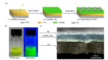
图1
Ag/CsPbBr3 QDs/ITO器件的制备与表征"
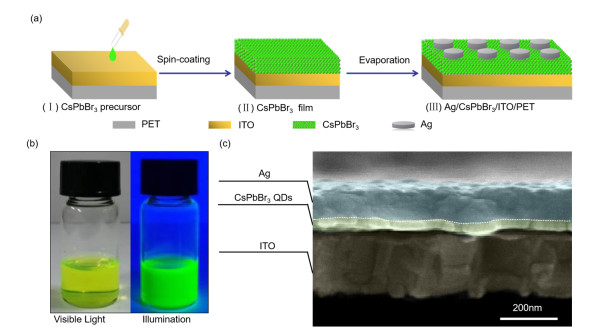
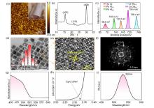
图2
CsPbBr3 QDs薄膜的表征"
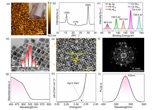
图3
Ag/CsPbBr3 QDs/ITO器件的阻变性能"
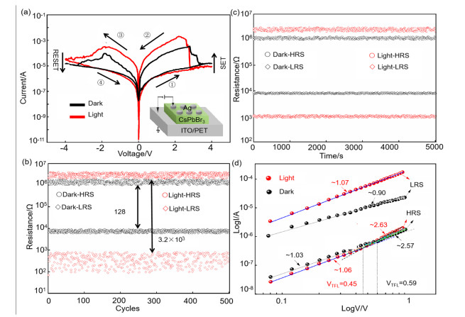
图4
36个存储单元在(a)暗态和(c)亮态条件下的ON/OFF彩色分布图(右侧为颜色刻度条),与(b)暗态和(d)亮态的VSET和VRESET分布图"
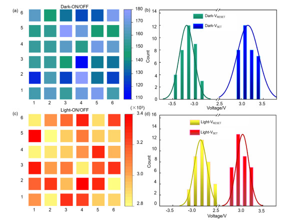
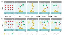
图5
Ag/CsPbBr3 QDs/ITO器件在(a)暗态和(b)亮态条件下阻变机制示意图"
| 1 |
Chang T. ; Chang K. ; Tsai T. ; Chu T. ; Sze S. Mater Today 2016, 19, 254.
doi: 10.1016/j.mattod.2015.11.009 |
| 2 |
Meijer G. Science 2008, 319, 1625.
doi: 10.1126/science.1153909 |
| 3 |
Ren S. ; Dong W. ; Tang H. ; Tang L. ; Li Z. ; Sun Q. ; Yang H. ; Yang Z. ; Zhao J. Appl. Surf. Sci. 2019, 488, 92.
doi: 10.1016/j.apsusc.2019.05.129 |
| 4 |
Ren S. ; Li Z. ; Tang L. ; Su X. ; Zhang H. ; Zhang G. ; Zhang H. ; Cao G. ; Zhao J. Adv. Electron. Mater. 2020, 6, 2000151.
doi: 10.1002/aelm.202000151 |
| 5 |
Nili H. ; Walia S. ; Balendhran S. ; Strukov D. ; Bhaskaran M. ; Sriram S. Adv. Funct. Mater. 2014, 24, 6733.
doi: 10.1002/adfm.201470279 |
| 6 |
Li S. ; Zeng H. ; Zhang S. ; Wei X. Appl. Phys. Lett. 2013, 102, 1636.
doi: 10.1063/1.4802209 |
| 7 |
Lin Y. ; Xu H. ; Wang Z. ; Cong T. ; Liu W. ; Ma H. ; Liu Y. Appl. Phys. Lett. 2017, 110, 193503.
doi: 10.1063/1.4983382 |
| 8 |
Wuttig M. ; Bhaskaran H. ; Taubner T. Nat. Photon 2017, 11, 465.
doi: 10.1038/NPHOTON.2017.126 |
| 9 |
He Z. ; Dai Y. ; Li X. ; Guo D. ; Liu Y. ; Huang X. ; Jiang J. ; Wang S. ; Zhu G. ; Zhang F. ; et al Small 2019, 15, 1804131.
doi: 10.1002/smll.201804131 |
| 10 |
Tan H. ; Liu G. ; Zhu X. ; Yang H. ; Chen B. ; Chen X. ; Shang J. ; Lu W. D. ; Wu Y. ; Li R.-W. Adv. Mater. 2015, 27, 2797.
doi: 10.1002/adma.201500039 |
| 11 |
Im J. ; Lee C. ; Lee J. ; Park S. ; Park N. Nanoscale 2011, 3, 4088.
doi: 10.1039/C1NR10867K |
| 12 |
Abdi-Jalebi M. ; Andaji-Garmaroudi Z. ; Cacovich S. ; Stavrakas C. ; Philippe B. ; Richter J. ; Alsari M. ; Booker E. ; Hutter E. ; Pearson A. ; et al Nature 2018, 555, 497.
doi: 10.1038/nature25989 |
| 13 |
Choi J. ; Han J. ; Hong K. ; Kim S. ; Jang H. Adv. Mater. 2018, 30, 1704002.
doi: 10.1002/adma.201704002 |
| 14 |
Wehrenfennig C. ; Eperon G. ; Johnston M. ; Snaith H. ; Herz L. Adv. Mater. 2014, 26, 1584.
doi: 10.1002/adma.201305172 |
| 15 |
Dong Q. F., Y. ; Shao Y. ; Mulligan P. ; Qiu J. ; Cao L. ; Huang J. Science 2015, 347, 967.
doi: 10.1126/SCIENCE.AAA5760 |
| 16 |
Zhao J. ; Wang P. ; Wei L. ; Liu Z. ; Fang X. ; Liu X. ; Ren D. ; Mai Y. Dalton Trans. 2015, 44, 16914.
doi: 10.1039/C5DT02388B |
| 17 |
Zhang F. ; Han B. ; Zeng H. J. Inorg. Mater. 2022, 2, 117.
doi: 10.15541/jim20210441 |
| 18 |
Dou L. ; Yang Y. ; You J. ; Hong Z. ; Chang W. ; Li G. ; Yang Y. Nat. Commun. 2014, 5, 5404.
doi: 10.1038/ncomms6404 |
| 19 |
Chen Y. ; Chen G. ; Zhou Z. ; Li X. ; Ma P. ; Li L. ; Yin W. ; Zeng H. ; Zou G. Adv. Funct. Mater. 2021, 31, 2101966.
doi: 10.1002/adfm.202101966 |
| 20 |
Lin K. ; Xing J. ; Quan L. ; de Arquer F. ; Gong X. ; Lu J. ; Xie L. ; Zhao W. ; Zhang D. ; Yan C. ; et al Nature 2018, 562, 245.
doi: 10.1038/s41586-018-0575-3 |
| 21 |
Han B. ; Yuan S. ; Cai B. ; Song J. ; Liu W. ; Zhang F. ; Fang T. ; Wei C. ; Zeng H. Adv. Funct. Mater. 2021, 31, 2011003.
doi: 10.1002/adfm.202011003 |
| 22 |
Chen J. ; Mukherjee S. ; Li W. ; Zeng H. ; Fischer R. Nat. Rev. Mater. 2022, 7, 677.
doi: 10.1038/s41578-022-00476-3 |
| 23 |
Wei C. ; Su W. ; Li J. ; Xu B. ; Shan Q. ; Wu Y. ; Zhang F. ; Luo M. ; Xiang H. ; Cui Z. ; Zeng H. Adv. Mater. 2022, 34, 2107798.
doi: 10.1002/adma.202107798 |
| 24 |
Zhang Q. ; Tavakoli M. ; Gu L. ; Zhang D. ; Tang L. ; Gao Y. ; Guo J. ; Lin Y. ; Leung S. ; Poddar S. ; et al Nat. Commun. 2019, 10, 727.
doi: 10.1038/s41467-019-08561-y |
| 25 |
Chin X. ; Cortecchia D. ; Yin J. ; Bruno A. ; Soci C. Nat. Commun. 2015, 6, 7383.
doi: 10.1038/ncomms8383 |
| 26 |
Chen Q. ; Zhang Y. ; Liu S. ; Han T. ; Chen X. ; Xu Y. ; Meng Z. ; Zhang G. ; Zheng X. ; Zhao J. ; et al Adv. Intell. Syst. 2020, 2, 2000122.
doi: 10.1002/aisy.202000122 |
| 27 |
Yoo E. ; Lyu M. ; Yun J. ; Kang C. ; Choi Y. ; Wang L. Adv. Mater. 2015, 27, 6170.
doi: 10.1002/adma.201502889 |
| 28 |
Choi J. ; Park S. ; Lee J. ; Hong K. ; Kim D. ; Moon C. ; Park G. ; Suh J. ; Hwang J. ; Kim S. ; et al Adv. Mater. 2016, 28, 6562.
doi: 10.1002/adma.201600859 |
| 29 |
Kim D. ; Tak Y. ; Kim W. ; Kim J. ; Kim J. ; Kim H. Adv. Mater. Interfaces 2017, 4, 1601035.
doi: 10.1002/admi.201601035 |
| 30 |
Hwang B. ; Lee J.-S. Adv. Mater. 2017, 29, 1701048.
doi: 10.1002/adma.201701048 |
| 31 |
Zhu X. ; Lee J. ; Lu W. Adv. Mater. 2017, 29, 1700527.
doi: 10.1002/adma.201700527 |
| 32 |
Zhou F. ; Liu Y. ; Shen X. ; Wang M. ; Yuan F. ; Chai Y. Adv. Funct. Mater. 2018, 28, 1800080.
doi: 10.1002/adfm.201800080 |
| 33 |
Xiao Z. ; Huang J. Adv. Electron. Mater. 2016, 2, 1600100.
doi: 10.1002/aelm.201600100 |
| 34 |
Chen S. ; Zhang Y. ; Zhao J. ; Mi Z. ; Zhang J. ; Cao J. ; Feng J. ; Zhang G. ; Qi J. ; Li J. ; et al Sci. Bull 2020, 65, 1643.
doi: 10.1016/j.scib.2020.05.020 |
| 35 |
Younis A. ; Lin C. ; Guan X. ; Shahrokhi S. ; Huang C. ; Wang Y. ; He T. ; Singh S. ; Hu L. ; Retamal J. ; et al Adv. Mater. 2021, 33, 2005000.
doi: 10.1002/adma.202005000 |
| 36 |
Futscher M. ; Mili J. Front. Energy Res. 2021, 9, 629074.
doi: 10.3389/fenrg.2021.629074 |
| 37 |
Wang Y. ; Lv Z. ; Liao Q. ; Shan H. ; Chen J. ; Zhou Y. ; Zhou L. ; Chen X. ; Roy V. ; Wang Z. ; et al Adv. Mater. 2018, 30, 1800327.
doi: 10.1002/adma.201800327 |
| 38 |
Yen M. ; Lee C. ; Liu K. ; Peng Y. ; Leng J. ; Chang T. ; Chang C. ; Tamada K. ; Lee Y. Nat. Commun. 2021, 12, 4460.
doi: 10.1038/s41467-021-24762-w |
| 39 |
Liu Q. ; Yue W. ; Li Y. ; Wang W. ; Xu L. ; Wang Y. ; Gao S. ; Zhang C. ; Kan H. ; Li C. Adv. Electron. Mater. 2021, 7, 2100366.
doi: 10.1002/aelm.202100366 |
| 40 |
Liu X. ; Ren S. ; Li Z. ; Guo J. ; Yi S. ; Yang Z. ; Hao W. ; Li R. ; Zhao J. Adv. Funct. Mater. 2022, 32, 2202951.
doi: 10.1002/adfm.202202951 |
| 41 |
Zhang G. ; Xu Y. ; Yang S. ; Ren S. ; Jiao Y. ; Wang Y. ; Ma X. ; Li H. ; Hao W. ; He C. ; Liu X. ; Zhao J. Nano Energy 2023, 106, 108074.
doi: 10.1016/j.nanoen.2022.108074 |
| 42 |
Du X. ; Wu G. ; Cheng J. ; Dang H. ; Ma K. ; Zhang Y. ; Tan P. ; Chen S. RSC Adv. 2017, 7, 10391.
doi: 10.1039/C6RA27665B |
| 43 |
Zhu Y. ; Cheng P. ; Shi J. ; Wang H. ; Liu Y. ; Xiong R. ; Ma H. ; Ma H. Adv. Electron. Mater. 2019, 6, 1900754.
doi: 10.1002/aelm.201900754 |
| 44 |
Wang F. ; Yu M. ; Chen X. ; Li J. ; Zhang Z. ; Li Y. ; Zhang G. ; Shi K. ; Shi L. ; Zhang M. ; et al SmartMat 2022, 4, e1135.
doi: 10.1002/smm2.1135 |
| 45 |
Wu G. ; Liang R. ; Ge M. ; Sun G. ; Zhang Y. ; Xing G. Adv. Mater. 2022, 34, 2105635.
doi: 10.1002/adma.202105635 |
| 46 |
Baranowski M. ; Plochocka P. Adv. Energy Mater. 2020, 1903659.
doi: 10.1002/aenm.201903659 |
| 47 |
Jong U. ; Yu C. ; Ri G. ; McMahon A. ; Harrison N ; Barnes P. ; Walsh A. J. Mater. Chem. A 2018, 6, 1067.
doi: 10.1039/C7TA09112E |
| 48 |
Cai H. ; Lao M. ; Xu J. ; Chen Y. ; Zhong C. ; Lu S. ; Hao A. ; Chen R. Ceram. Int. 2019, 45, 5724.
doi: 10.1016/j.ceramint.2018.12.038 |
| 49 |
Zhao X. ; Fan Z. ; Xu H. ; Wang Z. ; Xu J. ; Ma J. ; Liu Y. J. Mater. Chem. C 2018, 6, 7195.
doi: 10.1039/C8TC01844H |
| 50 |
Yoo E. ; Lyu M. ; Yun J. ; Kang C. ; Choi Y. ; Wang L. J. Mater. Chem. C 2016, 4, 7824.
doi: 10.1039/C6TC02503J |
| 51 |
Huang Y. ; Shen Z. ; Wu Y. ; Wang X. ; Zhang S. ; Shi X. ; Zeng H. RSC Adv. 2016, 6, 17867.
doi: 10.1039/C5RA22728C |
| [1] | 刘彬彬, 陈杨, 贾天赐, 陈辰, 吴章豪, 刘毓辉, 翟宇航, 马天舒, 王长擂. 羟基功能化分子工程消除二维相壁垒实现高效宽带隙及全钙钛矿叠层太阳能电池[J]. 物理化学学报, 2026, 42(1): 100128 - . |
| [2] | 梁英, 邓羽恒, 余士律, 程家豪, 宋嘉伟, 姚俊, 杨亦辰, 张万雷, 周文靖, 张欣, 沈文剑, 梁桂杰, 李彬, 彭勇, 胡润, 李望南. 机器学习辅助减反膜结构设计与界面修饰协同优化的高效稳定钙钛矿太阳能电池[J]. 物理化学学报, 2025, 41(9): 100098 - . |
| [3] | 戚洺瑄, 金斓煜, 姚宏鹤, 徐子鹏, 成腾, 陈棋, 朱城, 白阳. 钙钛矿太阳能电池在反向偏压下的电学失效及稳定性研究进展[J]. 物理化学学报, 2025, 41(8): 100088 - . |
| [4] | 李坚, 张毓, 闫融融, 孙开媛, 刘晓晴, 梁子尚, 焦忆楠, 卜晖, 陈欣, 赵晋津, 施剑林. 高效靶向示踪钙钛矿纳米系统光电增效抗肿瘤[J]. 物理化学学报, 2025, 41(5): 100042 - . |
| [5] | 马尧, 赵欣, 陈红旭, 魏薇, 沈亮. 钙钛矿薄单晶光电探测器的进展与展望[J]. 物理化学学报, 2025, 41(4): 100030 - . |
| [6] | 董鹏宇, 姜月, 杨正池, 刘立城, 李固, 文鑫洋, 王祯, 施信波, 周国富, 刘俊明, 高进伟. NbSe2纳米片优化钙钛矿太阳能电池的埋底界面[J]. 物理化学学报, 2025, 41(3): 100029 - . |
| [7] | 李尚华, 李玛琳, 迟茜文, 尹心, 罗招娣, 于吉红. 基于高离子迁移动力学的取向ZnQ分子筛保护层实现高稳定水系锌金属负极的构筑[J]. 物理化学学报, 2025, 41(1): 100003 - . |
| [8] | AhmedYameen, 封想想, 高远基, 丁洋, 龙操玉, HaiderMustafa, 李恒月, 李专, 黄誓成, SaidaminovMakhsud I., 阳军亮. 离子液体界面修饰的高效稳定FAPbI3钙钛矿太阳能电池[J]. 物理化学学报, 2024, 40(6): 2303057 - . |
| [9] | 冯炜程, 于景成, 杨溢澜, 郭宜阁, 邹庚, 刘晓菊, 陈洲, 董坤, 宋月锋, 汪国雄, 包信和. 调控双钙钛矿中高熵组分促进高温析氧反应[J]. 物理化学学报, 2024, 40(6): 2306013 - . |
| [10] | 李睿, 刘欢, 焦忆楠, 秦胜建, 孟婕, 宋佳钰, 闫融融, 苏航, 陈恒彬, 尚子璇, 赵晋津. 卤化物钙钛矿的单双向离子迁移[J]. 物理化学学报, 2024, 40(11): 2311011 - . |
| [11] | Faizan Muhammad, 赵国琪, 张天旭, 王啸宇, 贺欣, 张立军. 空位有序双钙钛矿A2BX6的弹性和热电性质的第一性原理研究[J]. 物理化学学报, 2024, 40(1): 2303004 - . |
| [12] | 胡荣, 韦丽云, 鲜靖林, 房光钰, 吴植傲, 樊淼, 郭家越, 李青翔, 刘凯思, 姜会钰, 徐卫林, 万骏, 姚永刚. 微波热冲快速制备二维多孔La0.2Sr0.8CoO3钙钛矿用于高效电催化析氧反应[J]. 物理化学学报, 2023, 39(9): 2212025 -0 . |
| [13] | 杨帅, 徐瑜歆, 郝子坤, 秦胜建, 张润鹏, 韩钰, 杜利伟, 朱紫洢, 杜安宁, 陈欣, 吴昊, 乔冰冰, 李坚, 王艺, 孙昺晨, 闫融融, 赵晋津. 高效医学传感钙钛矿材料研究进展[J]. 物理化学学报, 2023, 39(5): 2211025 -0 . |
| [14] | 文永涛, 李静, 高晓峰, 田聪聪, 朱昊, 余国木, 张晓俐, Park Hyesung, 黄福志. 控制碘化铅形貌两步连续刮涂法大面积制备甲脒基钙钛矿薄膜[J]. 物理化学学报, 2023, 39(2): 2203048 -0 . |
| [15] | 张涛, 龚思敏, 陈平, 陈琪, 陈立桅. 利用多氟丙烯酸酯添加剂提升准二维钙钛矿发光二极管性能[J]. 物理化学学报, 2023, 39(12): 2301024 - . |
|
||
