物理化学学报 >> 2025, Vol. 41 >> Issue (4): 100030.doi: 10.3866/PKU.WHXB202309045
所属专题: 新型光电功能材料
钙钛矿薄单晶光电探测器的进展与展望
马尧, 赵欣, 陈红旭, 魏薇, 沈亮*( )
)
- 吉林大学电子科学与工程学院, 集成光电子学国家重点实验室, 吉林大学未来科学国际合作联合实验室, 长春 130012
-
收稿日期:2023-09-28修回日期:2023-11-04录用日期:2023-11-06发布日期:2023-12-20 -
通讯作者:Email: shenliang@jlu.edu.cn; Tel.: +86-431-85168241 (沈亮) -
基金资助:吉林省国际科技合作项目(20210402079GH); 吉林省国际科技合作项目(20230402056GH); 吉林省第十九批创新创业人才项目(2023QN01); 吉林省科技发展计划(20220508037RC); 吉林大学研究生创新基金项目
Progress and Perspective of Perovskite Thin Single Crystal Photodetectors
Yao Ma, Xin Zhao, Hongxu Chen, Wei Wei, Liang Shen*()
- International Center of Future Science, State Key Laboratory of Integrated Optoelectronics, College of Electronic Science and Engineering, Jilin University, Changchun 130012, China
-
Received:2023-09-28Revised:2023-11-04Accepted:2023-11-06Published:2023-12-20 -
Contact:Email: shenliang@jlu.edu.cn; Tel.: +86-431-85168241 (Liang Shen) -
Supported by:the International Cooperation and Exchange Project of Jilin Province(20210402079GH); the International Cooperation and Exchange Project of Jilin Province(20230402056GH); the 19th Batch of Innovative and Entrepreneurial Talent Projects in Jilin Province(2023QN01); the Project of Science and Technology Development Plan of Jilin Province(20220508037RC); the Graduate Innovation Fund of Jilin University

摘要:
金属卤化物钙钛矿材料在光电探测领域具有突出的应用前景,但是多晶薄膜材料的晶界和缺陷问题,以及体单晶材料较厚的载流子传输距离限制了其性能。通过调控纵向尺寸制备的钙钛矿薄单晶材料理论上更适合光电探测,成为新型探测器领域的研究热点。本文介绍了钙钛矿单晶生长的结晶思路和薄单晶的制备工艺,回顾了钙钛矿薄单晶光电探测器领域的代表性工作,最后讨论了目前面临的问题和未来可能的发展方向。
引用本文
马尧, 赵欣, 陈红旭, 魏薇, 沈亮. 钙钛矿薄单晶光电探测器的进展与展望[J]. 物理化学学报, 2025, 41(4), 100030. doi: 10.3866/PKU.WHXB202309045
Yao Ma, Xin Zhao, Hongxu Chen, Wei Wei, Liang Shen. Progress and Perspective of Perovskite Thin Single Crystal Photodetectors[J]. Acta Phys. -Chim. Sin. 2025, 41(4), 100030. doi: 10.3866/PKU.WHXB202309045
图1
"
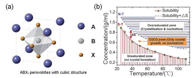
图2
"
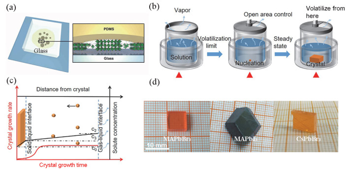
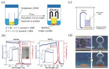
图3
"
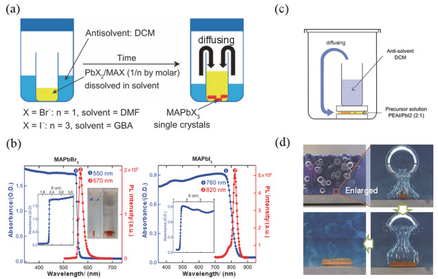
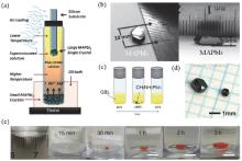
图4
"
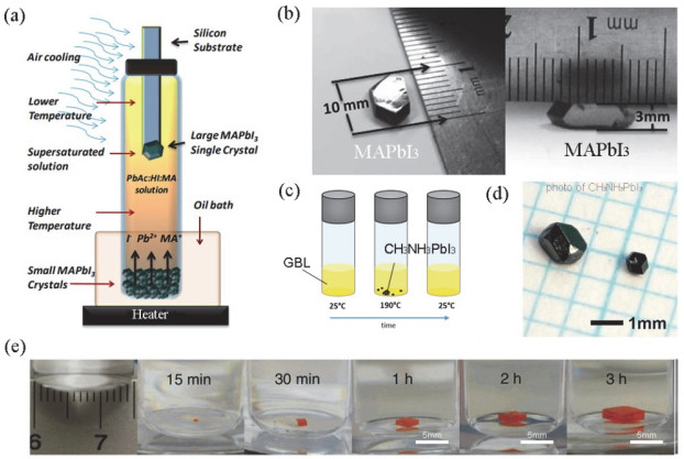
图5
"
图6
"
图7
"
图8
"
图9
"
图10
"
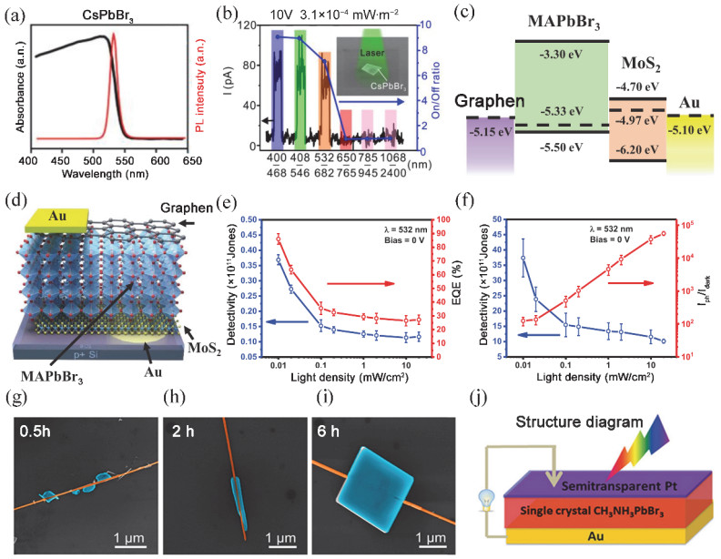
图11
"
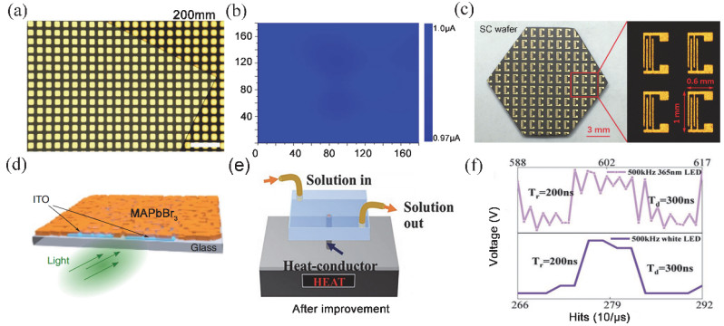
图12
"
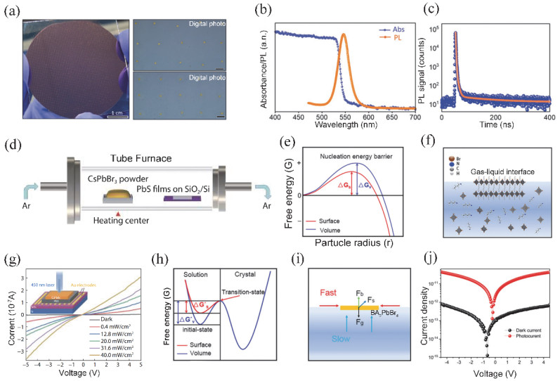
图13
"
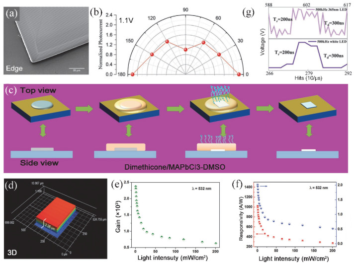
图14
"
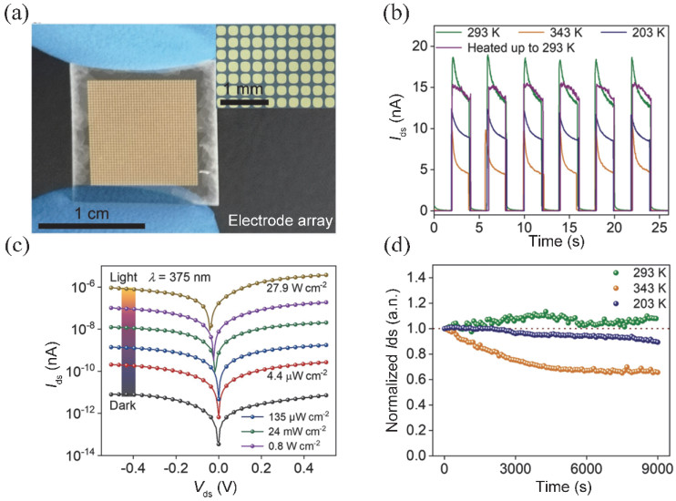
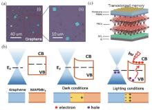
图15
"
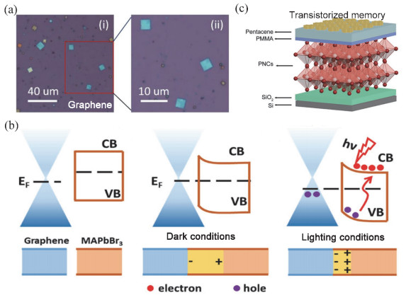
表1
不同单晶生长方法所得薄单晶"
| Growth method | Single crystal name | Lateral size | Vertical size | Ref. |
| Space-confined method | MAPbBr3 | Area 120 cm2 | 0.1–0.8 mm | |
| Space-confined method | MAPbBr3/MAPbI3 | – | 10–40 μm | |
| Space-confined method | MAPbX3 | Submillimeter-level | From nanometer to micron | |
| Surface tension controlled | MABX3 (B = Pb/Sn, X = Br/I) | 1 cm2 | 5–10 μm | |
| Surface tension controlled | (PEA)2PbI4 | Length 36 mm | – | |
| Vapor phase epitaxy | CsPbBr3/CsSnBr3 | centimeter-level | From nanometer to micron | |
| Vapor phase epitaxy | CsPbBr3 | 10 mm × 5 mm | 1–7 μm | |
| Top-down | MAPbX3 | – | 15–200 μm | |
| Lithography-assisted epitaxial | MAPbI3 | 5.5 cm × 5.5 cm | 0.6–100 μm | |
| Spin coating | MAPbBr3 | Length 3 μm–13 μm | – |
表2
器件类型及其性能参数"
| Device type | Growth method | Structure | Responsivity | Specific detectivity | Ref. |
| Photodiode | Chemical vapor deposition | Si/CsPbBr3 | 1.75 A∙W−1 | 1.41 × 10¹¹ Jones | |
| Photodiode | Space-confined method | Au/MoS2/MAPbBr3/Gt/Au | 368 mA∙W−1 | 3.74 × 10¹² Jones | |
| Photodiode | Anti-solvent method | CsPbBr3/ZnO | 3.5 × 10³ A∙W−1 | 6.6 × 10¹³ Jones | |
| Photodiode | Anti-solvent method | Pt/MAPbBr3 | ~4.5 mA∙W−1 | 7.1 × 10¹¹ Jones | |
| Photoconductor | Space-confined method | Si/Cs3Bi2I9 | ~3 mA∙W−1 | ~3 × 10¹¹ Jones | |
| Photoconductor | Crystal merge | ITO/MAPbBr3 | 4000 A∙W−1 | > 1013 Jones | |
| Photoconductor | Vapor phase epitaxy | CsPbBr3/PbS | 15 A∙W−1 | 2.65 × 10¹¹ Jones | |
| Photoconductor | Space-confined method | Au/BA2PbBr4/Au | ~45 mA∙W−1 | ~1012 Jones | |
| Photoconductor | Space-confined method | Graphene/MAPbBr3 | ~1017.1 A∙W−1 | ~2.02 × 10¹³ Jones | |
| Photoconductor | Vapor phase epitaxy | CsPbI3/Au | 32.8 A∙W−1 | 4.22 × 10¹² Jones |
| 1 |
doi: 10.1039/c3ee43161d |
| 2 |
doi: 10.1002/adma.201306281 |
| 3 |
doi: 10.1039/c5cp00448a |
| 4 |
doi: 10.1038/ncomms4586 |
| 5 |
doi: 10.1038/nphys3357 |
| 6 |
doi: 10.1038/nphoton.2015.156 |
| 7 |
doi: 10.1038/s41467-019-08768-z |
| 8 |
doi: 10.1002/smll.201903599 |
| 9 |
doi: 10.1021/acs.nanolett.1c00700 |
| 10 |
doi: 10.1002/smll.202001534 |
| 11 |
doi: 10.1126/science.abp8873 |
| 12 |
doi: 10.1038/s41586-023-06514-6 |
| 13 |
doi: 10.1038/s41377-020-0264-5 |
| 14 |
doi: 10.1038/s41566-022-01024-9 |
| 15 |
|
|
卢岳; 葛杨; 隋曼龄. 物理化学学报., 2022, 38 (5), 2007088.
doi: 10.3866/PKU.WHXB202007088 |
|
| 16 |
|
|
杨帅; 徐瑜歆; 郝子坤; 秦胜建; 张润鹏; 韩钰; 杜利伟; 朱紫洢; 杜安宁; 陈欣; 等. 物理化学学报., 2023, 39 (5), 2211025.
doi: 10.3866/PKU.WHXB202211025 |
|
| 17 |
|
|
张涛; 龚思敏; 陈平; 陈琪; 陈立桅. 物理化学学报, 2023, 39 (12), 2301024.
doi: 10.3866/PKU.WHXB202301024 |
|
| 18 |
doi: 10.3390/nano12234205 |
| 19 |
doi: 10.1021/acs.jpclett.1c02905 |
| 20 |
doi: 10.1002/adma.202208497 |
| 21 |
doi: 10.1002/adma.202205261 |
| 22 |
doi: 10.1039/c8cs00740c |
| 23 |
doi: 10.1039/c4mh00174e |
| 24 |
doi: 10.1002/adma.201502597 |
| 25 |
doi: 10.1002/anie.201511792 |
| 26 |
doi: 10.1039/c5cc06916e |
| 27 |
doi: 10.1038/s41467-017-00567-8 |
| 28 |
doi: 10.1038/s41467-021-21805-0 |
| 29 |
doi: 10.1016/j.mattod.2018.04.002 |
| 30 |
doi: 10.1038/ncomms8338 |
| 31 |
doi: 10.1002/admi.201800224 |
| 32 |
doi: 10.1039/c8ce01939h |
| 33 |
doi: 10.1016/j.scib.2021.06.016 |
| 34 |
doi: 10.1038/nmat4014 |
| 35 |
doi: 10.1126/science.aaa2725 |
| 36 |
doi: 10.1039/c7ce00240h |
| 37 |
doi: 10.1002/adma.201506292 |
| 38 |
doi: 10.1039/c4ce02106a |
| 39 |
doi: 10.1126/science.aaa5760 |
| 40 |
doi: 10.1038/srep11654 |
| 41 |
doi: 10.1038/ncomms8586 |
| 42 |
doi: 10.1002/adma.201601995 |
| 43 |
doi: 10.1002/aelm.201700655 |
| 44 |
doi: 10.1016/j.jcrysgro.2016.11.034 |
| 45 |
doi: 10.1002/adma.201602639 |
| 46 |
doi: 10.1038/s41467-017-02039-5 |
| 47 |
doi: 10.1021/jacs.6b09388 |
| 48 |
doi: 10.1021/acsenergylett.7b00468 |
| 49 |
doi: 10.1016/j.matt.2019.04.002 |
| 50 |
doi: 10.1002/adma.201702643 |
| 51 |
doi: 10.1021/jacs.7b07506 |
| 52 |
doi: 10.1007/s11426-017-9081-3 |
| 53 |
doi: 10.1039/c8tc00842f |
| 54 |
doi: 10.1038/s41586-020-2526-z |
| 55 |
doi: 10.1039/d2tc05392f |
| 56 |
doi: 10.1002/admi.202200912 |
| 57 |
doi: 10.1016/j.nantod.2020.101055 |
| 58 |
doi: 10.1039/c6tc02828d |
| 59 |
doi: 10.1126/sciadv.aat2390 |
| 60 |
doi: 10.1002/adma.202103010 |
| 61 |
doi: 10.1038/ncomms9724 |
| 62 |
doi: 10.1002/smll.202203565 |
| 63 |
doi: 10.1002/adfm.202209563 |
| 64 |
doi: 10.1088/1674-4926/42/11/112001 |
| 65 |
doi: 10.1039/d1tc00408e |
| 66 |
doi: 10.1002/adom.202100524 |
| 67 |
doi: 10.1002/smll.202000733 |
| 68 |
doi: 10.1002/adfm.202213360 |
| 69 |
doi: 10.1002/adfm.201909672 |
| 70 |
doi: 10.1016/j.scib.2017.08.022 |
| 71 |
doi: 10.1002/adfm.201905021 |
| 72 |
|
|
陈亮; 田中群. 物理化学学报, 2021, 37 (3), 2010065.
doi: 10.3866/PKU.WHXB202010065 |
|
| 73 |
doi: 10.1038/s41467-018-07177-y |
| 74 |
doi: 10.1038/s41566-023-01167-3 |
| 75 |
doi: 10.1126/sciadv.abc8844 |
| 76 |
doi: 10.1002/adma.202001998 |
| 77 |
doi: 10.1126/science.aba0893 |
| [1] | 刘彬彬, 陈杨, 贾天赐, 陈辰, 吴章豪, 刘毓辉, 翟宇航, 马天舒, 王长擂. 羟基功能化分子工程消除二维相壁垒实现高效宽带隙及全钙钛矿叠层太阳能电池[J]. 物理化学学报, 2026, 42(1): 100128 - . |
| [2] | 梁英, 邓羽恒, 余士律, 程家豪, 宋嘉伟, 姚俊, 杨亦辰, 张万雷, 周文靖, 张欣, 沈文剑, 梁桂杰, 李彬, 彭勇, 胡润, 李望南. 机器学习辅助减反膜结构设计与界面修饰协同优化的高效稳定钙钛矿太阳能电池[J]. 物理化学学报, 2025, 41(9): 100098 - . |
| [3] | 戚洺瑄, 金斓煜, 姚宏鹤, 徐子鹏, 成腾, 陈棋, 朱城, 白阳. 钙钛矿太阳能电池在反向偏压下的电学失效及稳定性研究进展[J]. 物理化学学报, 2025, 41(8): 100088 - . |
| [4] | 李坚, 张毓, 闫融融, 孙开媛, 刘晓晴, 梁子尚, 焦忆楠, 卜晖, 陈欣, 赵晋津, 施剑林. 高效靶向示踪钙钛矿纳米系统光电增效抗肿瘤[J]. 物理化学学报, 2025, 41(5): 100042 - . |
| [5] | 董鹏宇, 姜月, 杨正池, 刘立城, 李固, 文鑫洋, 王祯, 施信波, 周国富, 刘俊明, 高进伟. NbSe2纳米片优化钙钛矿太阳能电池的埋底界面[J]. 物理化学学报, 2025, 41(3): 100029 - . |
| [6] | 张宇航, 赵伟玮, 刘宏微, 吕俊鹏. 基于低维材料的自供电光电探测器研究进展[J]. 物理化学学报, 2025, 41(3): 100020 - . |
| [7] | 贺梦菲, 陈超, 唐月, 孟思, 王遵法, 王立煜, 行家宝, 张欣宇, 黄佳慧, 卢江波, 井红梅, 刘翔宇, 徐华. 外延生长具有厚度可调导电属性的非层状二维碲化锰纳米片用于p-型场效应晶体管和优异的接触电极[J]. 物理化学学报, 2025, 41(2): 100016 - . |
| [8] | 赵兴超, 李晓明, 刘明, 赵子进, 杨凯旋, 刘蓬天, 张皓岚, 李金泰, 马晓玲, 姚琪, 孙艳明, 张福俊. 倍增型全聚合物光电探测器及其在光电容积描记传感器上的应用[J]. 物理化学学报, 2025, 41(1): 100007 - . |
| [9] | AhmedYameen, 封想想, 高远基, 丁洋, 龙操玉, HaiderMustafa, 李恒月, 李专, 黄誓成, SaidaminovMakhsud I., 阳军亮. 离子液体界面修饰的高效稳定FAPbI3钙钛矿太阳能电池[J]. 物理化学学报, 2024, 40(6): 2303057 - . |
| [10] | 冯炜程, 于景成, 杨溢澜, 郭宜阁, 邹庚, 刘晓菊, 陈洲, 董坤, 宋月锋, 汪国雄, 包信和. 调控双钙钛矿中高熵组分促进高温析氧反应[J]. 物理化学学报, 2024, 40(6): 2306013 - . |
| [11] | 李睿, 刘欢, 焦忆楠, 秦胜建, 孟婕, 宋佳钰, 闫融融, 苏航, 陈恒彬, 尚子璇, 赵晋津. 卤化物钙钛矿的单双向离子迁移[J]. 物理化学学报, 2024, 40(11): 2311011 - . |
| [12] | Faizan Muhammad, 赵国琪, 张天旭, 王啸宇, 贺欣, 张立军. 空位有序双钙钛矿A2BX6的弹性和热电性质的第一性原理研究[J]. 物理化学学报, 2024, 40(1): 2303004 - . |
| [13] | 王鹤然, 陈凯, 伏硕, 王晧暄, 袁加轩, 胡星奕, 许文娟, 密保秀. 三种同分异构的双苯并吩噻嗪材料的合成、理论计算及光物理性质[J]. 物理化学学报, 2024, 40(1): 2303047 - . |
| [14] | 胡荣, 韦丽云, 鲜靖林, 房光钰, 吴植傲, 樊淼, 郭家越, 李青翔, 刘凯思, 姜会钰, 徐卫林, 万骏, 姚永刚. 微波热冲快速制备二维多孔La0.2Sr0.8CoO3钙钛矿用于高效电催化析氧反应[J]. 物理化学学报, 2023, 39(9): 2212025 -0 . |
| [15] | 杨帅, 徐瑜歆, 郝子坤, 秦胜建, 张润鹏, 韩钰, 杜利伟, 朱紫洢, 杜安宁, 陈欣, 吴昊, 乔冰冰, 李坚, 王艺, 孙昺晨, 闫融融, 赵晋津. 高效医学传感钙钛矿材料研究进展[J]. 物理化学学报, 2023, 39(5): 2211025 -0 . |
|
||