

物理化学学报 >> 2023, Vol. 39 >> Issue (10): 2306038.doi: 10.3866/PKU.WHXB202306038
所属专题: 北大纳米化学研究中心30周年专刊
廖珺豪1,2,3,4, 赵一萱1,3, 胡兆宁3,5, 补赛玉5, 陆琪3,6, 尚明鹏1,2,3, 贾开诚3, 裘晓辉4,*( ), 谢芹1,2,3,*(), 林立1,2,3,5,*(), 刘忠范1,2,3,*()
收稿日期:2023-06-26
录用日期:2023-07-24
发布日期:2023-08-07
通讯作者:
裘晓辉,谢芹,林立,刘忠范
E-mail:xhqiu@nanoctr.cn;xieqin-cnc@pku.edu.cn;linli-cnc@pku.edu.cn;zfliu@pku.edu.cn
基金资助:
Junhao Liao1,2,3,4, Yixuan Zhao1,3, Zhaoning Hu3,5, Saiyu Bu5, Qi Lu3,6, Mingpeng Shang1,2,3, Kaicheng Jia3, Xiaohui Qiu4,*(), Qin Xie1,2,3,*(), Li Lin1,2,3,5,*(), Zhongfan Liu1,2,3,*()
Received:2023-06-26
Accepted:2023-07-24
Published:2023-08-07
Contact:
Xiaohui Qiu, Qin Xie, Li Lin, Zhongfan Liu
E-mail:xhqiu@nanoctr.cn;xieqin-cnc@pku.edu.cn;linli-cnc@pku.edu.cn;zfliu@pku.edu.cn
Supported by:摘要:
为实现石墨烯在光通讯、光互联、太赫兹探测等电子和光电子领域的应用价值,需要在硅基衬底上得到大面积、均一且性能优异的石墨烯薄膜材料。而高品质石墨烯薄膜的制备衬底多为金属,因此制备的石墨烯薄膜不可避免地需要通过合适的转移方法,转移到目标应用衬底上。而转移过程通常会引入破损、褶皱和污染物,其原因之一是石墨烯转移和器件加工过程中表面反复涂覆和去除转移介质聚合物和光刻胶类聚合物。为避免反复涂覆与去除高分子聚合物,本文直接利用光刻胶作为转移介质,成功实现了石墨烯的洁净转移。同时,转移后石墨烯的电学性质得到明显改善,平均载流子迁移率可达6200 cm2·V−1·s−1。此方法可实现石墨烯等二维材料无损、洁净转移和高性能器件的构筑,将有助于推动二维材料在电子、光电子器件领域的应用。
廖珺豪, 赵一萱, 胡兆宁, 补赛玉, 陆琪, 尚明鹏, 贾开诚, 裘晓辉, 谢芹, 林立, 刘忠范. 光刻胶辅助的石墨烯晶圆无损转移[J]. 物理化学学报, 2023, 39(10), 2306038. doi: 10.3866/PKU.WHXB202306038
Junhao Liao, Yixuan Zhao, Zhaoning Hu, Saiyu Bu, Qi Lu, Mingpeng Shang, Kaicheng Jia, Xiaohui Qiu, Qin Xie, Li Lin, Zhongfan Liu. Crack-Free Transfer of Graphene Wafers via Photoresist as Transfer Medium[J]. Acta Phys. -Chim. Sin. 2023, 39(10), 2306038. doi: 10.3866/PKU.WHXB202306038
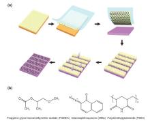
图1
光刻胶转移流程和其主要成分"
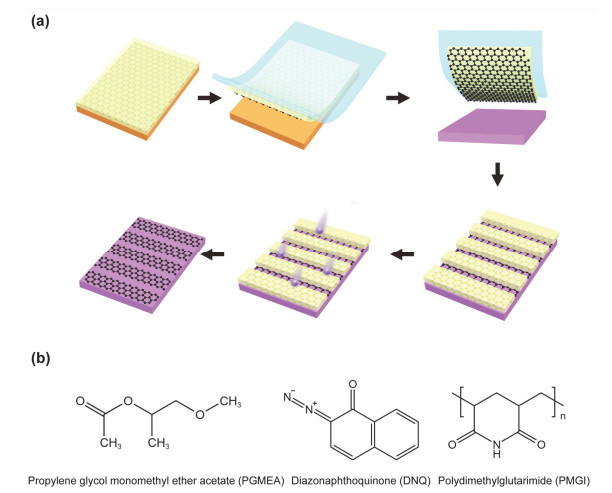
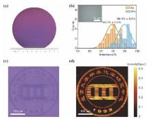
图2
完整和图案化石墨烯转移"
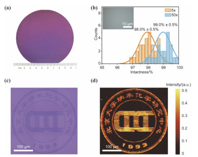
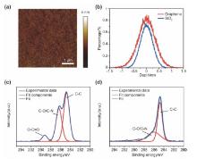
图3
石墨烯在SiO2/Si衬底上无褶皱洁净转移"
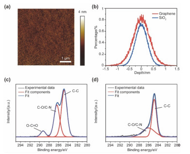
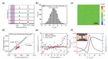
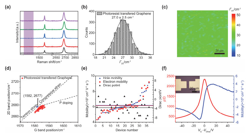
图4
转移后石墨烯拉曼和电学性能表征"
| 1 |
Lange K. ; Muller-Seitz G. ; Sydow J. ; Windeler A. Res. Policy 2013, 42 (3), 647.
doi: 10.1016/j.respol.2012.12.001 |
| 2 |
Yeh L. Y. ; Liao M. H. ; Chen C. H. ; Wu J. ; Lee J. Y. M. ; Liu C. W. ; Lee T. L. ; Liang M. S. IEEE Trans. Electron Devices 2009, 56 (11), 2848.
doi: 10.1109/ted.2009.2030542 |
| 3 |
Welser J. ; Hoyt J. L. ; Gibbons J. F. IEEE Electron. Device. Lett. 1994, 15 (3), 100.
doi: 10.1109/55.285389 |
| 4 |
Radisavljevic B. ; Kis A. Nat. Mater. 2013, 12 (9), 815.
doi: 10.1038/nmat3687 |
| 5 |
Dennard R. H. ; Gaensslen F. H. ; Yu H. N. ; Rideout V. L. ; Bassous E. ; Leblanc A. R. Proc. IEEE 1999, 87 (4), 668.
doi: 10.1109/jproc.1999.752522 |
| 6 |
Novoselov K. S. ; Geim A. K. ; Morozov S. V. ; Jiang D. ; Zhang Y. ; Dubonos S. V. ; Grigorieva I. V. ; Firsov A. A. Science 2004, 306 (5696), 666.
doi: 10.1126/science.1102896 |
| 7 |
Kretinin A. V. ; Cao Y. ; Tu J. S. ; Yu G. L. ; Jalil R. ; Novoselov K. S. ; Haigh S. J. ; Gholinia A. ; Mishchenko A. ; Lozada M. ; et al Nano Lett. 2014, 14 (6), 3270.
doi: 10.1021/nl5006542 |
| 8 |
Castro Neto A. H. ; Guinea F. ; Peres N. M. R. ; Novoselov K. S. ; Geim A. K. Rev. Mod. Phys. 2009, 81 (1), 109.
doi: 10.1103/revmodphys.81.109 |
| 9 |
Cao Y. ; Fatemi V. ; Fang S. ; Watanabe K. ; Taniguchi T. ; Kaxiras E. ; Jarillo-Herrero P. Nature 2018, 556 (7699), 43.
doi: 10.1038/nature26160 |
| 10 |
Giambra M. A. ; Miseikus V. ; Pezzini S. ; Marconi S. ; Montanaro A. ; Fabbri F. ; Sorianello V. ; Ferrari A. C. ; Coletti C. ; Romagnoli M. ACS Nano 2021, 15 (2), 3171.
doi: 10.1021/acsnano.0c09758 |
| 11 |
Goossens S. ; Navickaite G. ; Monasterio C. ; Gupta S. ; Piqueras J. J. ; Perez R. ; Burwell G. ; Nikitskiy I. ; Lasanta T. ; Galan T. ; et al Nat. Photonics 2017, 11 (6), 366.
doi: 10.1038/nphoton.2017.75 |
| 12 |
Marconi S. ; Giambra M. A. ; Montanaro A. ; Miseikis V. ; Soresi S. ; Tirelli S. ; Galli P. ; Buchali F. ; Templ W. ; Coletti C. ; et al Nat. Commun. 2021, 12 (1), 806.
doi: 10.1038/s41467-021-21137-z |
| 13 |
Liu C. H. ; Chang Y. C. ; Norris T. B. ; Zhong Z. H. Nat. Nanotechnol. 2014, 9 (4), 273.
doi: 10.1038/nnano.2014.31 |
| 14 |
Tian H. ; Yang Y. ; Xie D. ; Cui Y. L. ; Mi W. T. ; Zhang Y. G. ; Ren T. L. Sci. Rep. 2014, 4, 3598.
doi: 10.1038/srep03598 |
| 15 |
Wang M. ; Huang M. ; Luo D. ; Li Y. ; Choe M. ; Seong W. K. ; Kim M. ; Jin S. ; Wang M. ; Chatterjee S. ; et al Nature 2021, 596 (7873), 519.
doi: 10.1038/s41586-021-03753-3 |
| 16 |
Yuan G. W. ; Lin D. J. ; Wang Y. ; Huang X. L. ; Chen W. ; Xie X. D. ; Zong J. Y. ; Yuan Q. Q. ; Zheng H. ; Wang D. ; et al Nature 2020, 577 (7789), 204.
doi: 10.1038/s41586-019-1870-3 |
| 17 |
Chen T. A. ; Chuu C. P. ; Tseng C. C. ; Wen C. K. ; Wong H. S. P. ; Pan S. Y. ; Li R. T. ; Chao T. A. ; Chueh W. C. ; Zhang Y. F. ; et al Nature 2020, 579 (7798), 219.
doi: 10.1038/s41586-020-2009-2 |
| 18 |
Li Y. L. Z. ; Sun L. Z. ; Chang Z. H. ; Liu H. Y. ; Wang Y. C. ; Liang Y. ; Chen B. H. ; Ding Q. J. ; Zhao Z. Y. ; Wang R. Y. ; et al Adv. Mater. 2020, 32 (29), 2002034.
doi: 10.1002/adma.202002034 |
| 19 |
Zhang J. C. ; Lin L. ; Jia K. C. ; Sun L. Z. ; Peng H. L. ; Liu Z. F. Adv. Mater. 2020, 32 (1), 1903266.
doi: 10.1002/adma.201903266 |
| 20 |
Liu L. ; Li T. T. ; Ma L. ; Li W. S. ; Gao S. ; Sun W. J. ; Dong R. K. ; Zou X. L. ; Fan D. X. ; Shao L. W. ; et al Nature 2022, 605 (7908), 69.
doi: 10.1038/s41586-022-04523-5 |
| 21 |
Liu X. T. ; Zhang J. C. ; Wang W. D. ; Zhao W. ; Chen H. ; Liu B. Y. ; Zhang M. Q. ; Liang F. S. ; Zhang L. J. ; Zhang R. ; et al Nano Res. 2022, 15 (4), 3775.
doi: 10.1007/s12274-021-3922-x |
| 22 |
Ci H. N. ; Chen J. T. ; Ma H. ; Sun X. L. ; Jiang X. Y. ; Liu K. C. ; Shan J. Y. ; Lian X. Y. ; Jiang B. ; Liu R. J. ; et al Adv. Mater. 2022, 34 (51), 2206389.
doi: 10.1002/adma.202206389 |
| 23 |
Akinwande D. ; Huyghebaert C. ; Wang C. H. ; Serna M. I. ; Goossens S. ; Li L. J. ; Wong H. S. P. ; Koppens F. H. L. Nature 2019, 573 (7775), 507.
doi: 10.1038/s41586-019-1573-9 |
| 24 |
Gao L. B. ; Ni G. X. ; Liu Y. P. ; Liu B. ; Neto A. H. C. ; Loh K. P. Nature 2014, 505 (7482), 190.
doi: 10.1038/nature12763 |
| 25 |
Kim J. ; Park H. ; Hannon J. B. ; Bedell S. W. ; Fogel K. ; Sadana D. K. ; Dimitrakopoulos C. Science 2013, 342 (6160), 833.
doi: 10.1126/science.1242988 |
| 26 |
Qing F. Z. ; Zhang Y. F. ; Niu Y. T. ; Stehle R. ; Chen Y. F. ; Li X. S. Nanoscale 2020, 12 (20), 10890.
doi: 10.1039/d0nr01198c |
| 27 |
Leong W. S. ; Wang H. Z. ; Yeo J. J. ; Martin-Martinez F. J. ; Zubair A. ; Shen P. C. ; Mao Y. W. ; Palacios T. ; Buehler M. J. ; Hong J. Y. ; et al Nat. Commun. 2019, 10 (1), 867.
doi: 10.1038/s41467-019-08813-x |
| 28 |
Zhang Z. K. ; Du J. H. ; Zhang D. D. ; Sun H. D. ; Yin L. C. ; Ma L. P. ; Chen J. S. ; Ma D. G. ; Cheng H. M. ; Ren W. C. Nat. Commun. 2017, 8, 14560.
doi: 10.1038/ncomms14560 |
| 29 |
Zhao Y. X. ; Song Y. Q. ; Hu Z. N. ; Wang W. D. ; Chang Z. H. ; Zhang Y. ; Lu Q. ; Wu H. T. ; Liao J. H. ; Zou W. T. ; et al Nat. Commun. 2022, 13 (1), 4409.
doi: 10.1038/s41467-022-31887-z |
| 30 |
Hu Z. N. ; Li F. F. ; Wu H. T. ; Liao J. H. ; Wang Q. ; Chen G. ; Shi Z. F. ; Zhu Y. Q. ; Bu S. Y. ; Zhao Y. X. ; et al Adv. Mater. 2023, 35 (29), 2300621.
doi: 10.1002/adma.202300621 |
| 31 |
De Fazio D. ; Purdie D. G. ; Ott A. K. ; Braeuninger-Weimer P. ; Khodkov T. ; Goossens S. ; Taniguchi T. ; Watanabe K. ; Livreri P. ; Koppens F. H. L. ; et al ACS Nano 2019, 13 (8), 8926.
doi: 10.1021/acsnano.9b02621 |
| 32 |
Matsumae T. ; Fujino M. ; Suga T. ECS J. Solid State Sci. Technol. 2017, 6 (8), 512.
doi: 10.1149/2.0111708jss |
| 33 |
Song Y. Q. ; Gao Y. Q. ; Liu X. T. ; Ma J. ; Chen B. H. ; Xie Q. ; Gao X. ; Zheng L. M. ; Zhang Y. ; Ding Q. J. ; et al Adv. Mater. 2022, 34 (1), 2105851.
doi: 10.1002/adma.202105851 |
| 34 |
Lin Y. C. ; Lu C. C. ; Yeh C. H. ; Jin C. H. ; Suenaga K. ; Chiu P. W. Nano Lett. 2012, 12 (1), 414.
doi: 10.1021/nl203733r |
| 35 |
Matsumae T. ; Koehler A. D. ; Greenlee J. D. ; Anderson T. J. ; Baumgart H. ; Jernigan G. G. ; Hobart K. D. ; Kub F. J. ECS J. Solid State Sci. Technol. 2015, 4 (7), 190.
doi: 10.1149/2.0031507jss |
| 36 |
Lui C. H. ; Liu L. ; Mak K. F. ; Flynn G. W. ; Heinz T. F. Nature 2009, 462 (7271), 339.
doi: 10.1038/nature08569 |
| 37 |
Hu Z. N. ; Zhao Y. X. ; Zou W. T. ; Lu Q. ; Liao J. H. ; Li F. F. ; Shang M. P. ; Lin L. ; Liu Z. F. Adv. Funct. Mater. 2022, 32 (42), 2203179.
doi: 10.1002/adfm.202203179 |
| 38 |
Chang Z. ; Yang R. ; Wei Y. J. Mech. Phys. Solids 2019, 132, 103697.
doi: 10.1016/j.jmps.2019.103697 |
| 39 |
Lee J. E. ; Ahn G. ; Shim J. ; Lee Y. S. ; Ryu S. Nat. Commun. 2012, 3, 1024.
doi: 10.1038/ncomms2022 |
| 40 |
Petrone N. ; Dean C. R. ; Meric I. ; Van der Zande A. M. ; Huang P. Y. ; Wang L. ; Muller D. ; Shepard K. L. ; Hone J. Nano Lett. 2012, 12 (6), 2751.
doi: 10.1021/nl204481s |
| 41 |
Banszerus L. ; Schmitz M. ; Engels S. ; Dauber J. ; Oellers M. ; Haupt F. ; Watanabe K. ; Taniguchi T. ; Beschoten B. ; Stampfer C. Sci. Adv. 2015, 1 (6), 1500222.
doi: 10.1126/sciadv.1500222 |
| 42 |
Pezzini S. ; Miseikis V. ; Pace S. ; Rossella F. ; Watanabe K. ; Taniguchi T. ; Coletti C. 2D Mater. 2020, 7 (4), 041003.
doi: 10.1088/2053-1583/aba645 |
| 43 |
Wang L. ; Meric I. ; Huang P. Y. ; Gao Q. ; Gao Y. ; Tran H. ; Taniguchi T. ; Watanabe K. ; Campos L. M. ; Muller D. A. ; et al Science 2013, 342 (6158), 614.
doi: 10.1126/science.1244358 |
| 44 |
Du X. ; Skachko I. ; Barker A. ; Andrei E. Y. Nat. Nanotechnol. 2008, 3 (8), 491.
doi: 10.1038/nnano.2008.199 |
| 45 |
Ki D. K. ; Morpurgo A. F. Nano Lett. 2013, 13 (11), 5165.
doi: 10.1021/nl402462q |
| 46 |
Lee W. H. ; Park Y. D. Adv. Mater. Interfaces 2018, 5, 1700316.
doi: 10.1002/admi.201700316 |
| 47 |
Lee W. H. ; Park J. ; Kim Y. ; Kim K. S. ; Hong B. H. ; Cho K. Adv. Mater. 2011, 23 (30), 3460.
doi: 10.1002/adma.201101340 |
| 48 |
Gammelgaard L. ; Caridad J. M. ; Cagliani A. ; Mackenzie D. M. A. ; Petersen D. H. ; Booth T. J. ; Boggild P. 2D Mater. 2014, 1 (3), 035005.
doi: 10.1088/2053-1583/1/3/035005 |
| [1] | 霍春安, 邱圣杰, 梁青满, 耿碧君, 雷志超, 王干, 邹玉玲, 田中群, 杨扬. 光镊捕获和操控尺度极限的进展[J]. 物理化学学报, 2024, 40(1): 2303037 - . |
| [2] | 冀连连, 王现鹏, 张莹莹, 申学礼, 薛娣, 王璐, 王滋, 王文冲, 黄丽珍, 迟力峰. 有机-有机界面效应的原位及非原位研究[J]. 物理化学学报, 2024, 40(1): 2304002 - . |
| [3] | 徐美佳, 张宇琛, 朱一帆, 李昌林, 吴子昂, 周雄, 吴凯. Pd(100)氧化表面上低温丙烷氧化的活性相研究[J]. 物理化学学报, 2023, 39(10): 2305033 - . |
| [4] | 邵长香, 曲良体. 水的气-液相转变获取电能研究进展[J]. 物理化学学报, 2023, 39(10): 2306004 - . |
| [5] | 江吉周, 余良浪, 李方轶, 邓文明, 潘聪, 王海涛, 邹菁, 丁耀彬, 邓凤霞, 黄佳. 水蒸汽浴FeS2高效Fenton降解甲草胺[J]. 物理化学学报, 2023, 39(3): 2209033 -0 . |
| [6] | 汪茹, 刘志康, 严超, 伽龙, 黄云辉. 高安全锂离子电池复合集流体的界面强化[J]. 物理化学学报, 2023, 39(2): 2203043 -0 . |
| [7] | 刘若娟, 刘冰之, 孙靖宇, 刘忠范. 气相助剂辅助绝缘衬底上石墨烯生长:现状与展望[J]. 物理化学学报, 2023, 39(1): 2111011 -0 . |
| [8] | 曹冲, 张裴, 曹立冬, 刘铭鑫, 宋玉莹, 陈鹏, 黄啟良, 韩布兴. 液滴在超疏水植物叶面的沉积:实验和分子动力学模拟[J]. 物理化学学报, 2022, 38(12): 2207006 - . |
| [9] | 贺文娅, 程虎虎, 曲良体. 烯碳纤维基能源器件的研究进展[J]. 物理化学学报, 2022, 38(9): 2203004 - . |
| [10] | 曹晓辉, 侯成义, 李耀刚, 李克睿, 张青红, 王宏志. 基于MXenes的功能纤维的制备及其在智能可穿戴领域的应用[J]. 物理化学学报, 2022, 38(9): 2204058 - . |
| [11] | 张勇, 陆浩杰, 梁晓平, 张明超, 梁华润, 张莹莹. 蚕丝基智能纤维及织物:潜力、现状与未来展望[J]. 物理化学学报, 2022, 38(9): 2103034 - . |
| [12] | 夏洲, 邵元龙. 湿法纺制石墨烯纤维:工艺、结构、性能与智能应用[J]. 物理化学学报, 2022, 38(9): 2103046 - . |
| [13] | 吴昆杰, 张永毅, 勇振中, 李清文. 碳纳米管纤维的连续制备及高性能化[J]. 物理化学学报, 2022, 38(9): 2106034 - . |
| [14] | 温烨烨, 任明, 邸江涛, 张锦. 烯碳材料在人工肌肉领域的应用进展[J]. 物理化学学报, 2022, 38(9): 2107006 - . |
| [15] | 俞宏伟, 李实, 李金龙, 朱韶华, 孙成珍. 气驱油油气混相过程的界面传质特性及其分子机制[J]. 物理化学学报, 2022, 38(5): 2006061 - . |
|
||
